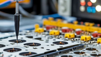
Global PCB sourcing is no longer a simple search for the lowest factory quote. Buyers now evaluate design quality, material traceability, testing, delivery stability, and environmental controls. The challenge is practical: a board may look perfect on screen but fail after thermal cycling, vibration, or repeated assembly.
Industry data shows why disciplined sourcing matters. Prismark’s 2024 PCB market outlook estimated global PCB revenue at roughly US$73 billion, with growth supported by automotive electronics, data centers, and artificial intelligence hardware. IPC’s 2024 industry outlook also highlighted continuing concerns about supply-chain resilience, skilled labor, and regional manufacturing capacity. These conditions affect every buyer, from a startup ordering 200 prototypes to an OEM planning monthly production.
Small details matter. Copper thickness, surface finish, impedance control, and solder-mask clearance can change both cost and reliability. A supplier’s ISO 9001 certificate helps, but it does not replace factory audits, first-article inspection, or measurable test records. Ask for cross-section images, test coupons, material certificates, and clear acceptance criteria. Make pcb decisions with evidence, not attractive product photos.
Experience also teaches a harder lesson: the cheapest quote can become the most expensive option. Delayed samples, unclear engineering changes, or inconsistent plating may disrupt an entire launch. This guide examines ten practical ways to make pcb sourcing more reliable for global buyers. It considers engineering communication, supplier verification, quality control, logistics, and responsible production. No method removes every risk. Good procurement simply makes those risks visible earlier.

10 Best Ways to Make PCB for Global Buyers?
Choose the Right PCB Manufacturing Method for Your Product
The right PCB method depends on risk, volume, geometry, and delivery pressure. A two-layer FR-4 board suits many control products, while HDI supports compact devices with fine-pitch components. Flexible circuits fit moving assemblies, but they demand tighter bend-radius control and more careful handling. Choose the structure after reviewing the enclosure, current load, thermal path, and assembly process.
IPC’s 2023 World PCB Production Report indicates that Asia produced about 90% of global printed circuit boards. That concentration can support competitive pricing, but distance adds freight, customs, and communication risks. For ten prototype boards, quick-turn fabrication may be sensible. For 100,000 units, panelization, automated inspection, and stable material sourcing matter more. A low unit price can hide expensive rework.
Ask for controlled impedance data, stack-up drawings, test coverage, and traceability records. Check whether the factory follows recognized quality systems and can provide material certificates. For high-density designs, request a design-for-manufacturing review before tooling. Small annular rings look efficient on a screen. They can become yield problems in production. The Global Electronics Association has repeatedly identified supply-chain resilience and regional capacity as major electronics concerns in recent industry outlooks. That means dual sourcing may deserve consideration, even when the second supplier costs more. No method is perfect. A prototype decision made without future volume data often needs revision.

10 Best Ways to Make PCB for Global Buyers
Prepare PCB Designs and Files for International Production
Preparing a PCB for global production requires more than exporting Gerber files. A reliable design package should include the schematic, approved layout, board stackup, drill data, fabrication notes, and revision history. Validate footprints against real component drawings, especially connector locations and mechanical holes. Keep it explicit. Small errors travel.
Use design-rule checks before release, then review clearance, trace width, copper weight, and impedance requirements with the intended fabricator. Confirm whether metric or imperial units are used. Include a clear board outline and a panelization preference when volume production is expected. Your material choices should match temperature, voltage, and environmental requirements. Do not assume every factory interprets notes identically.
A complete assembly package also needs the bill of materials, centroid file, polarity marks, assembly drawings, and approved substitutions. Check part availability before freezing the design; an elegant circuit can still fail when one component is unavailable worldwide. I have seen missing pin-one markings create avoidable inspection delays. That lesson remains uncomfortable. Add test points, inspection criteria, and acceptance tolerances where possible. Review every filename and revision number, then open the files on another computer before sending them. A final independent review often catches the mistake the designer no longer sees.
10 Best Ways to Make PCB for Global Buyers
Select Materials, Layer Structures, and Surface Finishes
A reliable PCB begins with the right material, not the lowest quoted price. Standard glass-reinforced epoxy suits many control boards and moderate-temperature devices. High-frequency circuits may need materials with controlled dielectric properties. I have seen poor material choices create impedance drift, heat damage, and early delamination. Confirm the operating temperature, signal speed, copper thickness, and expected service life before production.
Layer structure affects both performance and cost. A four-layer board can provide dedicated power and ground planes, reducing noise and improving routing space. However, adding layers is not always better. It may increase drilling complexity and inspection requirements. Surface finish also matters. Electroless nickel immersion gold supports fine-pitch assembly and storage stability. Lead-free leveling finishes can reduce cost but may require tighter process control. Select the finish according to solderability, contact wear, shelf life, and local environmental requirements.
Tips: Ask for material certificates, stackup drawings, impedance data, and finish thickness records. Request a small trial batch when the design is new. Inspect solder joints under magnification, especially near thermal pads and fine-pitch components. Do not assume the first design is perfect. Review warpage, plating consistency, and assembly yield after testing. A practical supplier should explain limitations clearly and provide traceable inspection results.
| No. | PCB Manufacturing Approach | Recommended Base Material | Typical Layer Structure | Suitable Surface Finish | Best For | Main Advantages | Important Buyer Considerations |
|---|---|---|---|---|---|---|---|
| 1 | Standard FR-4 Rigid PCB | Glass-reinforced epoxy laminate, commonly rated around Tg 130–170°C | 1–4 layers for basic designs; 4–8 layers for higher routing density | HASL, lead-free HASL, ENIG, or OSP | General electronics, control boards, appliances, and industrial products | Balanced mechanical strength, electrical insulation, availability, and cost | Confirm board thickness, copper weight, dielectric spacing, and the required flammability rating, such as UL 94 V-0 where applicable. |
| 2 | High-Tg FR-4 PCB | High-temperature glass-reinforced epoxy laminate, typically with Tg above 170°C | 4–12 layers, depending on routing, power, and thermal requirements | ENIG, ENEPIG, OSP, or lead-free HASL | Automotive electronics, industrial controls, and lead-free reflow assemblies | Improved resistance to thermal expansion and repeated high-temperature processing | A high Tg value does not automatically guarantee high thermal reliability; review Z-axis expansion, thermal cycling, and copper construction. |
| 3 | High-Speed or Low-Loss PCB | Low-loss laminate with controlled dielectric constant and dissipation factor | 4–16 layers with impedance-controlled signal, reference, and power planes | ENIG or immersion silver; choose the finish according to signal, assembly, and storage needs | High-speed digital links, radio-frequency circuits, networking, and data systems | Supports controlled impedance, reduced dielectric loss, and improved signal integrity | Specify the target impedance, stack-up, trace geometry, roughness requirements, dielectric tolerance, and test method before production. |
| 4 | Metal-Core LED PCB | Aluminum core with a dielectric insulation layer; copper core may be selected for higher heat spreading | Usually single-layer or two-layer; multilayer metal-core structures are also possible | HASL, lead-free HASL, ENIG, or OSP | LED lighting, power converters, motor drivers, and heat-generating circuits | Transfers heat from components toward a metal backing plate or heat sink | Check thermal conductivity, dielectric breakdown voltage, core thickness, flatness, mounting method, and thermal interface design. |
| 5 | Flexible Polyimide PCB | Polyimide film with rolled-annealed or electrodeposited copper | 1–4 layers; multilayer flex designs are possible for compact assemblies | ENIG, immersion tin, or OSP, depending on contact and assembly requirements | Wearables, cameras, displays, hinges, compact sensors, and moving assemblies | Lightweight, bendable, space-saving, and suitable for dynamic or static flexing | Define bend radius, bend cycles, stiffener locations, coverlay openings, copper type, and the direction of repeated flexing. |
| 6 | Rigid-Flex PCB | Combination of FR-4 rigid sections and polyimide flexible sections | Rigid multilayer zones connected by one or more flexible layers | ENIG, ENEPIG, immersion tin, or OSP | Aerospace, medical instruments, robotics, and products with limited interconnect space | Reduces connectors and cable assemblies while improving packaging reliability | Control flex-to-rigid transitions, coverlay design, bend radius, stiffeners, copper distribution, and assembly handling. |
| 7 | HDI Microvia PCB | FR-4, high-Tg FR-4, or low-loss laminate matched to electrical requirements | Sequentially built 1+N+1, 2+N+2, or higher-order structures with laser microvias | ENIG or ENEPIG; OSP may be used where suitable for assembly and storage conditions | Mobile electronics, compact computing devices, fine-pitch packages, and dense modules | Enables finer routing, smaller vias, higher interconnect density, and reduced board size | Review microvia diameter, aspect ratio, via stacking or staggering, pad sizes, resin filling, and sequential lamination capability. |
| 8 | Heavy-Copper PCB | FR-4, high-Tg FR-4, or metal-core construction with increased copper thickness | 1–6 layers; copper may range from approximately 3 oz to more than 10 oz on selected layers | Lead-free HASL, ENIG, or other finish compatible with the assembly process | Power supplies, battery systems, industrial drives, automotive power, and high-current distribution | Provides higher current capacity, improved heat spreading, and stronger power interconnections | Consider etching limits, conductor spacing, via current capacity, copper balance, thermal stress, and the required finished copper thickness. |
| 9 | Fine-Pitch Assembly PCB | High-quality FR-4, high-Tg FR-4, or low-loss laminate as required by the circuit | 2–12 layers with fine traces, small pads, and controlled solder-mask registration | ENIG or ENEPIG for flat, uniform pads; OSP may be suitable for compatible processes | BGA, QFN, CSP, and other fine-pitch surface-mount assemblies | Supports flat pads, accurate component placement, and reliable solder-joint formation | Set solder-mask clearance, via-in-pad requirements, pad finish thickness, coplanarity, inspection method, and assembly capability. |
| 10 | Prototype and Quick-Turn PCB | Standard FR-4 for most prototypes; polyimide or metal-core for specialized validation | 1–4 layers for simple prototypes; 4–8 layers for early product-level testing | HASL for economical through-hole work, ENIG for flat SMD pads, or OSP for selected short-cycle builds | Engineering validation, functional testing, pilot production, and design iteration | Shorter development cycles and lower initial tooling or purchasing commitment | Use production-intent materials and stack-up when possible; verify drill sizes, tolerances, impedance, and finish before design validation. |
Choosing a PCB supplier for global buyers requires more than comparing the lowest quotation. Suppliers differ in layer capability, material control, testing, and delivery stability. Request a clear capability sheet covering board size, layer count, copper thickness, impedance control, and minimum trace spacing. Ask for recent inspection records, process certifications, and sample reports. Reliable suppliers explain limitations instead of promising everything.
Cost comparisons should include engineering fees, tooling, electrical testing, packaging, freight, taxes, and possible redesign work. A two-layer prototype may look inexpensive, but multilayer boards with controlled impedance can change the budget sharply. Get matching quotations with the same Gerber files, stack-up, surface finish, and order quantity. Production capacity matters too. Check monthly output, equipment maintenance, holiday schedules, and backup processes. Ask whether automated optical inspection, flying-probe testing, or X-ray inspection suits your design.
A local supplier may reduce communication delays. A distant supplier may offer stronger volume pricing or advanced HDI production. Neither option is automatically safer. I would not trust a polished website alone. One overlooked tolerance can create weeks of delay. Small pilot orders, video audits, and signed quality criteria provide better evidence. Still, even careful sourcing can miss a packaging issue or shipping disruption. That risk deserves a contingency plan, not optimistic wording.
10 Best Ways to Make PCB for Global Buyers?
Verify Quality, Compliance, Packaging, and International Delivery
A reliable PCB supplier should show more than attractive samples. Request inspection records, material certificates, solderability results, and electrical test data. Check whether each board has traceable lot numbers, revision codes, and inspection dates. Review the production process, including drilling, plating, assembly, and final testing. Small details matter. A clean prototype can still hide weak copper adhesion or unstable dimensions. Ask for sample photos under clear lighting, not only polished catalog images. Compliance documents should match the exact materials and finished product. Confirm declarations for restricted substances, safety requirements, and destination-market rules. Rules can change, so old paperwork deserves another question.
Packaging protects quality after production ends. Use moisture-barrier bags, desiccant, humidity cards, and ESD-safe materials where required. Add foam protection without pressing delicate components or connectors. Cartons should resist stacking and ordinary handling. Request a drop-test record for larger shipments. International delivery also needs accurate invoices, product descriptions, quantities, weights, and customs classifications. Confirm delivery terms, insurance responsibility, tracking, and a backup transport plan. Delays often begin with one missing document.
Tips: Ask for a pre-shipment inspection before paying the balance. Compare carton labels with the packing list. Keep a retained sample for future checks. No checklist is perfect. Recheck the first shipment manually, even when the supplier appears experienced.