Choosing a China top quick turn flex PCB manufacturer requires more than comparing delivery dates or online ratings. Flexible circuits must bend repeatedly, fit narrow spaces, and maintain stable electrical performance. A reliable supplier should demonstrate practical experience with polyimide materials, copper thickness, stiffeners, coverlay, and controlled impedance designs.
This guide examines how manufacturers handle quick turn flex PCB projects from prototype review to final inspection. Real capability appears in small details. Can the engineering team identify a tight bend radius before fabrication? Can it explain why a solder pad needs reinforcement? Can it provide traceable material records and clear test reports? These questions reveal more than attractive marketing language.
Speed matters. Accuracy matters more.
A strong manufacturer usually combines responsive communication, documented process controls, and experienced technicians. Useful evidence may include sample panels, inspection images, first-article reports, and feedback from comparable industries. Independent certifications can support credibility, but certificates alone do not prove consistent workmanship. Production records and transparent corrective actions offer stronger evidence.
Not every fast supplier is the right supplier. Some may promise aggressive lead times without explaining design limitations. That deserves careful review. Prototype success can also hide weaknesses during volume production. Therefore, this article considers capability, reliability, engineering support, quality inspection, and total project risk. It also highlights practical questions buyers should ask before selecting a Chinese flex PCB partner. The goal is not to praise one factory blindly, but to identify dependable performance through evidence, communication, and repeatable results.

A quick-turn flex PCB manufacturer in China is a production partner built for short lead times, not merely a factory with spare capacity. It reviews Gerber files, flex stack-ups, bend zones, and material availability before accepting an order. Typical prototypes may ship within three to ten working days. The exact schedule depends on layer count, stiffeners, surface finish, and testing needs. Speed has limits.
Grand View Research reported that the global flexible electronics market reached about USD 29.7 billion in 2023, with strong growth expected through 2030. This expansion increases demand for compact, lightweight circuit assemblies. A capable Chinese manufacturer should therefore combine rapid quoting with controlled engineering review. DFM checks should identify narrow traces, sharp bend corners, unsuitable coverlay openings, and weak adhesive areas. IPC-2223 guidance is commonly used when evaluating flexible circuit design and mechanical reliability.
Experience matters during urgent builds. Engineers may recommend polyimide thickness changes or adjust copper treatment for repeated bending. They should also provide impedance data, dimensional records, and electrical test results. IPC’s standards and technical test methods offer a recognized framework for process verification, although compliance claims still require evidence from the actual lot. Do not trust “fast delivery” alone. A rushed order can reveal incomplete drawings, unavailable materials, or poor change control. One practical weakness remains: some suppliers quote quickly but explain risks poorly. Buyers should request a documented timeline, first-article criteria, and inspection records before production begins.
Copper foil thickness is a key material specification in flexible PCB production. Thinner foil supports lighter, more flexible circuits, while thicker foil is commonly selected when higher current capacity or improved durability is required. The values below represent commonly specified copper foil thicknesses used in flex PCB design and fabrication.
Copper foil thickness is shown in micrometers (µm). Final material selection depends on current requirements, bend conditions, stack-up design, and manufacturing capability.
China’s quick-turn flex PCB process begins with complete design data. Engineers review Gerber files, drill files, stack-up details, and material requirements. They check bend zones, trace spacing, minimum radii, and stiffener locations. A short design review often prevents expensive rework.
Production starts by cleaning and preparing the flexible copper-clad laminate. Circuit patterns are transferred onto the copper surface through imaging. Etching removes unwanted copper, while controlled drilling creates vias and component holes. Plating then strengthens the conductive paths. Coverlay is applied over exposed circuits, leaving only the required pads open. Some designs also receive polyimide stiffeners near connectors.
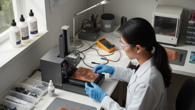
Inspection is continuous. Technicians use automated optical inspection to find shorts, opens, and pattern defects. Electrical testing checks every net against the approved data. They may also inspect bending samples by hand. Small details matter. A connector edge can feel rough. A tight bend may fail after repeated movement. Quick-turn production is not simply faster production; it depends on clear files, available materials, and disciplined scheduling. In practice, the first design revision is not always perfect. A missing bend note or unclear tolerance can delay fabrication more than the factory itself. Experienced manufacturers confirm these points before releasing panels, although communication can still be improved. Samples are finally cleaned, packed with moisture protection, and prepared for shipment from China.
China Top Quick Turn Flex PCB Manufacturer?
Key Capabilities of a Top Chinese Flex PCB Manufacturer
A top Chinese flex PCB manufacturer combines speed with disciplined engineering. Quick-turn production should begin with a clear design review. Engineers check bend radius, copper thickness, layer alignment, and coverlay clearance. They also examine drawings for missing tolerances. Small errors can delay an entire build.
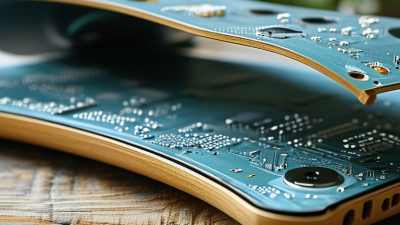
Strong manufacturers offer flexible material choices for different operating conditions. Polyimide substrates support repeated bending and compact assemblies. Rolled copper improves flexibility in dynamic applications. Controlled impedance designs require accurate stack-up planning and careful etching. Laser drilling, precision routing, and fine-line imaging help produce dense circuits. The factory should also maintain clean work areas and calibrated inspection equipment.
Reliable production depends on more than modern machines. Experienced teams use design-for-manufacturing feedback before fabrication. They record material batches, process settings, and inspection results. Electrical testing, visual checks, and dimensional measurements should be documented. Traceability matters.
No factory gets every first article perfect. A capable supplier admits this and corrects problems openly. Engineers may request a revised drawing or a tighter bend test. That extra discussion can prevent field failures. Customers should ask for sample reports, process controls, and realistic lead times. Fast service is useful, but predictable quality matters more.
| Capability | Typical Quick-Turn Range | Why It Matters | Common Industry Reference |
|---|---|---|---|
| Prototype turnaround | Approximately 3–7 working days for standard single- or double-sided flex PCBs after design approval | Supports rapid engineering validation and short product-development cycles | Lead time depends on layer count, material availability, tooling, testing, and order quantity |
| Production turnaround | Typically 7–15 working days for standard multilayer flex PCB orders | Provides a practical balance between delivery speed, process control, and production volume | Actual timing varies according to stack-up, surface finish, component assembly, and inspection requirements |
| Layer construction | 1–2 layers for fastest prototypes; 4–8 layers commonly available for advanced designs | Enables compact routing, higher circuit density, and integration of more functions into limited spaces | Multilayer capability should be confirmed against the required bend areas and stack-up |
| Flexible base materials | Polyimide film is standard; polyester and adhesive-free materials may also be available | Material selection affects thermal stability, flexibility, signal performance, and service life | Polyimide is widely used for applications requiring repeated bending or elevated temperature resistance |
| Finished board thickness | Approximately 0.10–0.30 mm for many standard flex constructions | Thin profiles help reduce package size and support tight mechanical routing | Final thickness depends on copper weight, coverlay, stiffeners, adhesive layers, and total layer count |
| Fine-line routing | Approximately 0.075–0.10 mm trace width and spacing for suitable designs | Allows high-density interconnects in cameras, displays, wearables, sensors, and compact electronics | Achievable dimensions depend on copper thickness, etching control, registration, and board geometry |
| Copper thickness | Commonly 0.5–2 oz finished copper; heavier copper is available for selected designs | Determines current-carrying capacity, thermal behavior, flexibility, and minimum bend radius | Current requirements should be evaluated using trace width, copper thickness, temperature rise, and bend conditions |
| Surface finishes | ENIG, immersion tin, immersion silver, and OSP are commonly specified options | Surface finish affects solderability, contact reliability, shelf life, and fine-pitch assembly performance | Finish selection should consider contact use, soldering process, storage time, and cost |
| Stiffener integration | Polyimide, FR-4, and stainless-steel stiffeners can be added to selected areas | Improves connector insertion, component support, dimensional stability, and assembly handling | Stiffener thickness and placement must be defined in the mechanical drawing |
| Coverlay and solder-mask control | Coverlay is commonly used to protect flexible conductors; liquid solder mask may be used in selected areas | Protects copper from oxidation, contamination, and mechanical damage while preserving bend zones | Opening accuracy and coverlay registration are critical around pads and dynamic-bend areas |
| Controlled impedance | Single-ended and differential impedance structures can be designed when stack-up data is controlled | Supports signal integrity in high-speed display, camera, computing, and communication applications | Requires accurate dielectric thickness, trace geometry, copper thickness, and impedance testing |
| Mechanical bending capability | Static bend designs commonly use a bend radius of at least 6× the finished thickness; dynamic designs require a larger radius | Helps prevent conductor cracking, delamination, and premature failure during installation or repeated motion | The exact radius depends on layer count, copper type, grain direction, neutral axis, and cycle requirements |
| Electrical testing | Open-and-short testing is standard; flying-probe or fixture testing may be selected according to volume | Detects manufacturing defects before shipment and improves prototype reliability | Additional options may include impedance testing, microsection analysis, and dimensional inspection |
| Quality standards | Manufacturing can be controlled to IPC-6013 and IPC-A-600 requirements when specified | Creates consistent acceptance criteria for flexible printed board fabrication and visual quality | The applicable class, revision, and customer-specific requirements should be stated on the purchase documentation |
| Design-for-manufacturing support | Gerber, ODB++, drill files, stack-up drawings, bend-zone data, and fabrication notes are commonly reviewed | Early engineering feedback can reduce rework, clarify tolerances, and shorten prototype approval time | A complete data package should define materials, tolerances, stiffeners, coverlay openings, bend areas, and testing needs |
Note: The figures above represent typical industry capability ranges for quick-turn flexible PCB production. Actual specifications and lead times depend on the approved design, material availability, order quantity, testing requirements, and manufacturing process.
Evaluating a quick turn flex PCB manufacturer requires more than comparing delivery dates. Inspect the supplier’s engineering process, material control, and testing records. A capable team should review bend radius, copper thickness, layer count, and adhesive selection before quoting. Ask for a sample cross-section or microsection report. It can reveal voids, uneven plating, and weak layer bonding. Small details matter.
Speed depends on preparation, not promises. Request a clear timeline for engineering review, tooling, fabrication, inspection, and shipping. A trustworthy manufacturer should explain possible delays before production begins. Ask whether standard materials are stocked locally. Confirm how design changes affect the schedule. Fast production without controlled inspection creates expensive surprises. That happens more often than expected.
Reliability needs measurable evidence. Check continuity testing, insulation testing, automated optical inspection, and final dimensional records. For high-flex applications, request bend-cycle data under conditions close to actual use. Review traceability from raw material to finished panel. Industry certifications and documented corrective actions also show process maturity. However, paperwork alone is not proof. I would still compare a pilot lot with the approved sample, because minor wrinkles or exposed copper may appear only after repeated bending. A practical supplier will discuss these weaknesses openly, rather than presenting every result as perfect.
Quick-turn flex PCBs help engineers test compact electronic designs without waiting through long production cycles. Their thin structure supports repeated bending, folding, and movement inside tight assemblies. These boards are common in wearable devices, medical instruments, cameras, and portable measurement equipment. A prototype can reveal routing problems before expensive tooling begins.
In medical equipment, flex circuits connect sensors, displays, and small control modules within limited spaces. Their lightweight construction can improve comfort in wearable monitors. In cameras, they route signals between moving lenses, buttons, and image modules. Printers and scanners also use them around hinges and sliding mechanisms. Automotive interiors apply flex PCBs to displays, lighting controls, and steering-wheel interfaces.
Industrial devices use them where vibration and limited installation space create wiring challenges. Engineers often select polyimide materials for heat resistance and dimensional stability. However, a quick prototype is not automatically production-ready. Bend radius, copper thickness, adhesive choice, and connector stress still require testing. I have seen designs pass electrical checks but fail after repeated folding. That mistake is avoidable. Clear stack-up drawings and realistic flex-cycle tests improve reliability. A capable quick-turn manufacturer should review tolerances, drilling details, surface finish, and inspection requirements before fabrication. Some early designs also need changes after assembly, especially when stiffeners block natural movement. This is where practical manufacturing feedback matters.