How to Choose the Best PCB Board Fabrication Method for Your Project in 2025
As the demand for advanced electronics continues to rise, the importance of choosing the right PCB board fabrication method has never been more critical. According to a report by MarketsandMarkets, the global PCB market size is projected to grow from $70.76 billion in 2020 to $92.48 billion by 2025, highlighting the increasing reliance on printed circuit boards across various industries, including automotive, consumer electronics, and telecommunications. This growth emphasizes the necessity for project managers and engineers to carefully evaluate their fabrication options to ensure efficiency, cost-effectiveness, and high-quality outputs.
Dr. Linda Chen, a leading expert in PCB technologies, states, "The choice of fabrication method not only affects the quality and performance of the final product but also influences the overall production timeline and costs." Her insights reflect the complex decision-making involved in PCB board fabrication, where factors such as material selection, manufacturing techniques, and design specs come into play. In 2025, as innovative technologies emerge and drive the evolution of PCB production methods, understanding these variables will be crucial for professionals striving to keep pace with industry advancements. This guide aims to equip you with the knowledge needed to make informed decisions regarding PCB board fabrication methods that align with your project objectives.

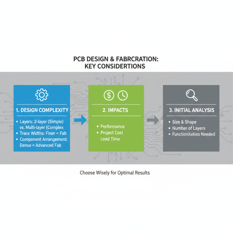
Determining Project Requirements: Analyzing PCB Complexity and Functionality
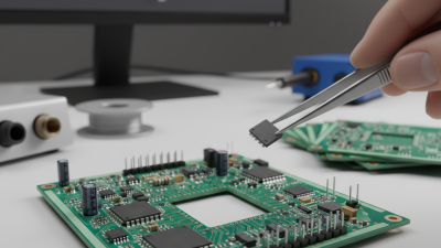
When embarking on a project that involves PCB design and fabrication, understanding the complexity and functionality of the PCB is essential for selecting the right fabrication method. The intricacy of your PCB can significantly impact not only the performance but also the cost and lead time of your project. For instance, a simple two-layer board may suffice for basic applications, while more complex designs with multiple layers, finer trace widths, and intricate component arrangements may require advanced fabrication techniques. Thus, a comprehensive analysis of the design requirements, including the size, number of layers, and needed functionalities, should be conducted at the outset.
Moreover, the functionality of the PCB plays a critical role in the determination of the fabrication method. If your project involves high-frequency signals or requires precise signal integrity, a method that can ensure minimal electromagnetic interference and optimal thermal management will be necessary. On the other hand, a project focusing on rapid prototyping might prioritize a faster, less expensive fabrication process, even if it compromises on performance. Understanding these nuances allows project leaders to align their manufacturing choices with technical needs, ensuring that the final product meets both performance expectations and budget constraints.
Evaluating Fabrication Methods: Comparing Subtractive, Additive, and Hybrid Techniques
When selecting a PCB board fabrication method for your project, understanding the differences between subtractive, additive, and hybrid techniques is crucial. Subtractive methods, such as traditional etching, involve removing material from a blank board to create the desired circuit pattern. This approach is commonly used for standard PCBs and benefits from established processes and equipment. However, the limitations in design flexibility and potential waste of materials can be significant drawbacks, especially for complex or custom layouts.
Additive methods, on the other hand, build up the PCB layer by layer, applying materials only where needed. This technique allows for intricate designs and can significantly reduce material waste. Furthermore, additive methods can facilitate the integration of components directly onto the PCB, leading to lower manufacturing costs for certain applications. Nonetheless, these techniques may require more advanced technology and can have longer production times when compared to subtractive methods.
Hybrid methods combine both subtractive and additive processes, offering a balance between material efficiency and production flexibility. By leveraging the strengths of each technique, hybrid fabrication can cater to complex designs while minimizing waste. This approach is particularly beneficial for industries that demand high precision and customization, making it an appealing option for modern PCB manufacturing in 2025. As project requirements evolve, understanding these fabrication methods will help engineers make informed decisions to optimize their designs.
Evaluation of PCB Fabrication Methods in 2025
This chart compares the popularity of different PCB fabrication methods in 2025. Subtractive methods remain the most popular, followed by additive and hybrid techniques.
Cost Analysis: Understanding Material Costs, Labor, and Production Scale Impact
When selecting the best PCB board fabrication method for your project, understanding the impact of material costs, labor, and production scale is vital. The choice of materials plays a significant role not only in the performance of the PCB but also in the overall budget. High-performance materials may lead to enhanced functionality but can significantly increase costs. Evaluating the specific needs of your project is crucial—if high-frequency performance is not essential, opting for a more basic material can help control expenses.
Labor costs also need to be considered, especially when evaluating different fabrication methods. Processes that require skilled labor or intensive manual work may drive up the total cost of production. Automation can help reduce labor costs but may require a larger upfront investment in machinery. It's essential to find a balance between quality and cost, ensuring that the method chosen aligns with the project timeline and labor availability.
Tips: Always consult with your fabrication partner to get a clear breakdown of costs associated with different materials and processes. Additionally, consider running a cost-benefit analysis for small batches versus large-scale productions, as economies of scale can significantly affect the overall pricing structure. By carefully analyzing all these factors, you can make an informed decision that aligns with both your budget and project requirements.
How to Choose the Best PCB Board Fabrication Method for Your Project in 2025
| Fabrication Method |
Material Cost per Unit ($) |
Labor Cost per Unit ($) |
Production Scale (Units per Month) |
Total Cost per Month ($) |
| Standard Laminated PCB |
50 |
20 |
1000 |
70000 |
| Flex PCB |
70 |
25 |
500 |
47500 |
| Rigid-Flex PCB |
90 |
30 |
300 |
36000 |
| High Frequency PCB |
120 |
40 |
200 |
32000 |
| Through-Hole PCB |
45 |
15 |
1500 |
90000 |
Lead Times and Production Capacity: Choosing Response Times for Timely Delivery
When selecting a PCB board fabrication method for your project, one crucial aspect to consider is lead times and production capacity. Understanding the response times of different manufacturers can significantly impact your project's timeline and success. If you need a fast turnaround, be sure to choose a fabrication method that aligns with your delivery requirements. Some methods can expedite specific processes, while others may introduce delays due to complexity or resource availability.
Tips for timely delivery include setting clear deadlines and communicating them with your manufacturer from the outset. Establishing a realistic timeline based on your project’s needs will help ensure smooth production flow. Moreover, consider keeping a buffer time in your planning phase to account for unexpected delays, especially if your project demands rapid prototyping or a quick market launch.
Additionally, it's essential to assess each method's production capacity to ensure it aligns with your project's scale. Some fabrication methods are better suited for high-volume production, while others may work best for smaller batches. Understanding these capabilities can help you make informed decisions and choose a fabrication approach that meets your project's specifications and timelines.
Sustainability Considerations: Assessing Eco-Friendly Practices in PCB Manufacturing
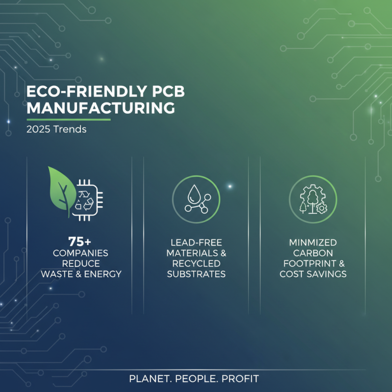
In 2025, sustainability has become a pivotal factor in selecting PCB board fabrication methods. As environmental concerns grow, the PCB manufacturing industry is gradually adopting eco-friendly practices. Reports indicate that over 75% of PCB manufacturing companies are implementing measures to reduce waste and energy consumption, aligning with global sustainability goals. Techniques such as employing lead-free materials, utilizing recycled substrates, and minimizing the carbon footprint of production processes are not only beneficial for the planet but often result in long-term cost savings for businesses.
When assessing eco-friendly practices in PCB manufacturing, it's essential to consider the source of raw materials and the energy efficiency of the fabrication process. Opting for suppliers who prioritize sustainable practices can significantly enhance a project's environmental impact. For example, choosing manufacturers that utilize solar energy or wind power in their facilities can contribute to a drastic reduction in greenhouse gas emissions.
**Tips:** Always request information on the life cycle assessment of PCB materials. This can provide insight into the environmental impact from production to disposal. Additionally, consider collaborating with companies that have received sustainability certifications, ensuring that your project aligns with eco-friendly principles. As the industry continues to evolve, prioritizing sustainability will not only enhance your project's credibility but also contribute to a greener future.