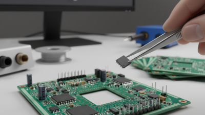
How to Choose the Right PCB Ways for Your Electronic Projects
When embarking on electronic projects, one of the critical decisions you will face is selecting the right PCB ways for your design. PCB ways, or the routes through which electrical signals travel on a printed circuit board, significantly impact both the functionality and performance of the project. Understanding how to choose the appropriate PCB ways is essential for optimizing layout efficiency, signal integrity, and overall reliability.
In this guide, we will delve into various factors that influence the selection of PCB ways, such as the size of the components, the complexity of the circuit, and the potential for electromagnetic interference. By carefully considering these elements, you can ensure that your PCB design not only meets the technical requirements of your project but also aligns with your production capabilities and cost constraints. Whether you are a hobbyist exploring new electronic designs or a seasoned engineer tackling complex applications, understanding the intricacies of PCB ways will be instrumental in the success of your electronic endeavors.
Understanding PCB Types: Rigid, Flexible, and Rigid-Flex Options
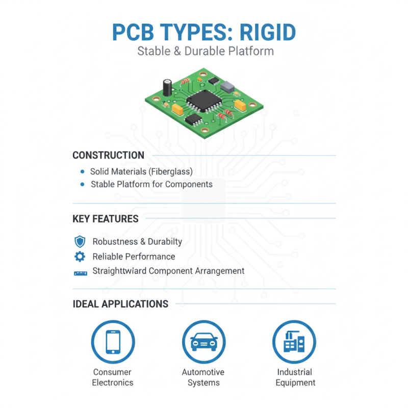
When selecting a suitable PCB for your electronic projects, understanding the different types available is crucial. Rigid PCBs are the most traditional and commonly used type. They are made from solid materials such as fiberglass and are designed to provide a stable platform for components. Due to their robustness, rigid PCBs are ideal for applications where durability and reliability are paramount, such as in consumer electronics or automotive systems. Their design allows for a straightforward arrangement of components, making them a go-to choice for many standard projects.
On the other hand, flexible PCBs offer advantages in terms of versatility and space efficiency. Made from materials that can bend and conform to different shapes, these boards are perfect for compact devices where a rigid design would be impractical. They facilitate designs that demand innovative layout solutions, such as in wearable technology or medical devices. Rigid-flex PCBs combine both rigid and flexible elements, allowing designers to create complex circuits that can withstand both structural demands and movements. This hybrid approach is beneficial in applications requiring a delicate balance between flexibility and strength, making it a compelling choice for modern electronic designs. Each type of PCB serves unique purposes, and understanding these options will guide you in making the best choice for your project.
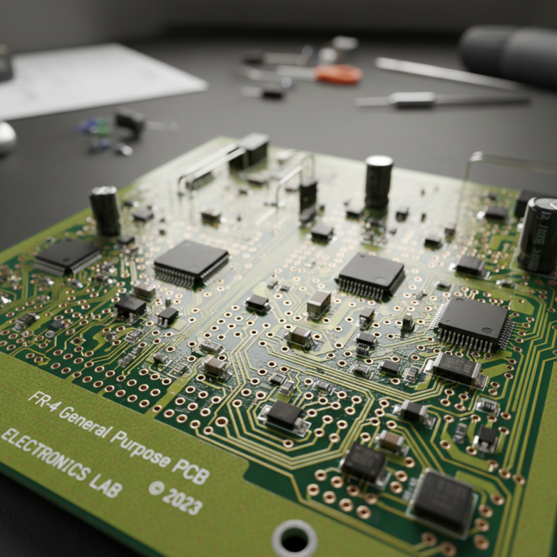
Key Considerations for PCB Material Selection: FR-4 vs. Rogers
When selecting the appropriate PCB material for your electronic projects, two prominent options often come to the forefront: FR-4 and Rogers materials. FR-4 is a widely used composite of woven fiberglass cloth and epoxy resin, known for its excellent mechanical properties and cost-effectiveness. It provides good insulation, is readily available, and works well for a variety of general-purpose applications. Ideal for lower-frequency circuits and standard temperature environments, FR-4 is the go-to choice for many hobbyists and manufacturers alike.
On the other hand, Rogers materials are specifically designed for high-frequency applications. They offer superior performance in terms of dielectric constant stability and lower loss factor, making them suitable for advanced RF and microwave designs. The properties of Rogers materials allow for less signal degradation over distance, leading to better performance in applications such as antennas and high-speed data transmission. However, they tend to be more expensive than FR-4, making it essential to assess the requirements of your project carefully to determine which material aligns best with your performance needs and budget considerations.
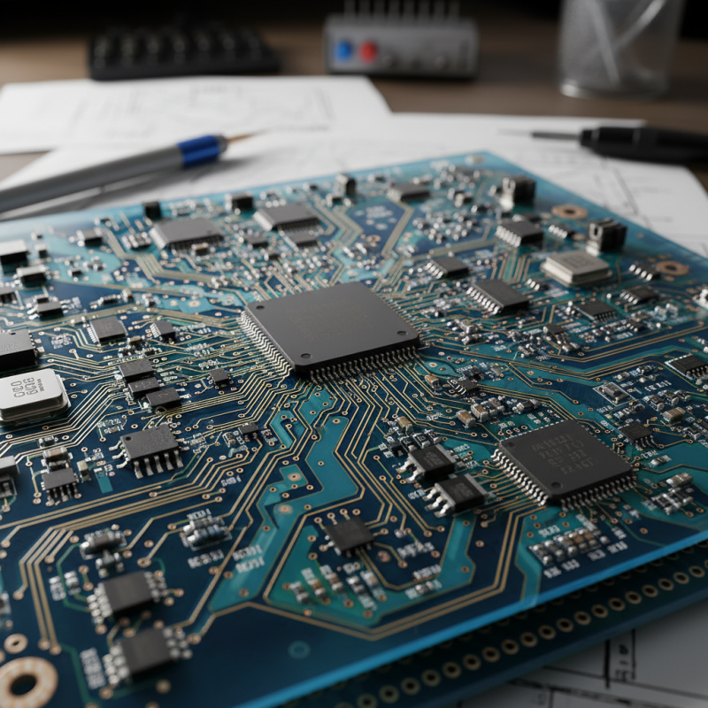
Evaluating Layer Count: Determining Your Project's Complexity Needs
When choosing the right PCB for your electronic projects, evaluating the layer count is crucial in determining the complexity and functionality of your design. Generally, a single-layer PCB is suitable for simple, low-density circuits, such as basic consumer electronics or toys. However, as project requirements grow, particularly in terms of functionality and density, multi-layer PCBs become increasingly necessary. Reports from industry analysts indicate that the global demand for multi-layer PCBs is expected to exceed 31 billion dollars by 2025, highlighting their importance in advanced applications.
The layer count directly impacts not only the physical space available for components but also influences signal integrity, thermal management, and manufacturing costs. For instance, a four-layer PCB can significantly enhance the performance of high-frequency circuits by improving signal routing and minimizing electromagnetic interference. Additionally, as the Internet of Things (IoT) continues to proliferate, the trend leans toward more complicated designs with higher layer counts, accommodating complex features like wireless communication and multifunctionality. Data shows that over 70% of IoT devices utilize PCBs with a minimum of two layers, emphasizing the need to understand layer requirements before commencing design.
Importance of Trace Width and Spacing: Ensuring Signal Integrity
When designing electronic projects, understanding the significance of trace width and spacing is crucial for ensuring signal integrity. Trace width directly affects the resistance and current-carrying capacity of a printed circuit board (PCB). A wider trace can handle higher currents, reducing voltage drop and minimizing heat generation. Conversely, if the trace is too narrow for the required current, it may overheat, leading to potential failures. Therefore, careful calculation of the trace width based on the expected current load is essential to prevent performance issues and increase the longevity of the PCB.
Equally important is the spacing between traces. As electronic devices become increasingly compact, the risk of crosstalk—unwanted transfer of signals between nearby traces—becomes a significant concern. Maintaining adequate spacing helps mitigate interference and maintain signal integrity, especially in high-frequency applications. Designers must balance trace width and spacing based on the operating frequency of the signals and the overall layout of the PCB. Proper planning in these aspects not only enhances performance but also increases the reliability of the entire electronic system.
How to Choose the Right PCB Ways for Your Electronic Projects - Importance of Trace Width and Spacing: Ensuring Signal Integrity
| Parameter |
Recommended Values |
Impact on Signal Integrity |
| Trace Width |
0.25 mm - 5 mm |
Wider traces reduce resistance and improve current capacity. |
| Trace Spacing |
0.2 mm - 0.5 mm |
Adequate spacing prevents crosstalk and maintains signal integrity. |
| Max Current Carrying Capacity |
Depends on trace width |
Ensures traces can handle expected current without overheating. |
| Impedance Control |
50 Ohm or 75 Ohm |
Match impedance to minimize signal reflection and loss. |
| Layer Stackup |
Single-sided, double-sided, multi-layer |
Affects trace routing options, signal integrity, and EMI performance. |
Cost Analysis: Balancing Quality and Budget in PCB Manufacturing
When embarking on electronic projects, understanding the cost implications of different PCB ways is vital to ensure a balance between quality and budget. According to a report by IPC, the global electronics manufacturing services market reached approximately $480 billion in 2020, with PCB fabrication costs accounting for a significant portion. A well-structured budget that takes into account material costs, manufacturing processes, and the complexity of the design can prevent unexpected financial burdens.
One key consideration in your cost analysis is the choice between standard and advanced materials. While advanced materials may enhance performance and longevity, they also come at a higher cost. A study from Research and Markets indicates that using high-frequency PCB materials may increase costs by 10-15%, which is critical to factor in when designing for specific applications. Additionally, labor costs associated with intricate designs can triple if using manual assembly versus automated processes.
**Tips:** Always start with a clear project scope to identify the specific materials and manufacturing types required. Engage with multiple suppliers to understand price ranges and potential hidden costs. Finally, consider prototyping as a way to test designs before full production—this can save both time and money in the long run.