How to Create a Perfect PCB Prototype: Tips for Efficient Design and Production
In the rapidly evolving world of electronics, creating a flawless PCB prototype is paramount for ensuring the success of any project. As John Smith, a leading expert in PCB design, wisely stated, "The quality of your PCB prototype directly impacts the performance and reliability of your final product." This encapsulates the importance of meticulous design and production processes in the realm of printed circuit boards.
To achieve the desired results, designers must marry innovation with strategic planning, utilizing advanced design software and materials while maintaining a keen eye on production efficiency. The art of developing an exceptional PCB prototype lies not only in technical expertise but also in understanding the intricacies of the manufacturing process. This guide aims to equip engineers and designers with essential tips that will streamline their journey from concept to production, ultimately leading to high-quality prototypes that stand the test of time.
Adopting a thoughtful approach to PCB prototyping is crucial in today’s competitive market. With the right strategies in place, professionals can enhance their design’s functionality and reduce time-to-market, paving the way for groundbreaking advancements in technology.
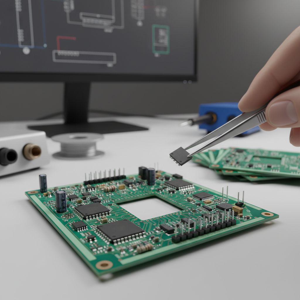
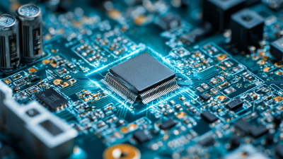
Understanding the Basics of PCB Prototyping and Its Importance
PCB prototyping is a crucial step in the development of electronic devices. By creating a physical model of a printed circuit board,
designers can test and validate the functionality of their circuits before committing to mass production. This process allows for the identification of
design flaws and potential issues, reducing the risk of costly mistakes and ensuring that the final product meets the intended specifications.
Understanding the basics of PCB prototyping begins with selecting appropriate materials and methods for your design.
Factors such as the intended application, complexity of the circuit, and cost-effectiveness play significant roles in this selection process.
Techniques like rapid prototyping and the use of software tools for simulation can greatly enhance the efficiency of design iterations.
Ensuring adequate testing and validation during this phase is essential, as it lays the foundation for a reliable and functional end product.
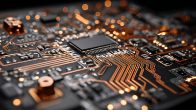
Key Considerations for Efficient PCB Design and Layout Techniques
When designing a perfect PCB prototype, the layout and design techniques play a crucial role in the overall efficiency and performance of the final product. Paying attention to component placement is vital. Arrange related components close together to minimize the length of the connections, which can help reduce noise and improve signal integrity. Additionally, consider the thermal requirements of your circuit. Placing heat-generating components away from sensitive ones will help prevent overheating and ensure reliable performance.
Another key consideration in PCB design is the routing of traces. Aim for shorter, more direct paths; this not only enhances signal quality but also simplifies the manufacturing process. Utilize ground planes to minimize electromagnetic interference. Additionally, don't overlook the importance of using adequate trace width to handle the required current without overheating.
Tips for efficient PCB design include adopting a modular approach where possible, allowing for easier changes and enhancements in the future. Regularly reviewing design rules and utilizing simulation tools can help identify potential issues early in the design phase, leading to a smoother production process.
PCB Prototype Design Efficiency
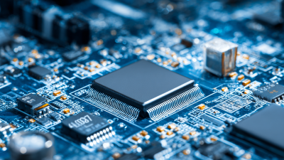
Selecting the Right Materials and Components for PCB Prototypes
When it comes to creating an effective PCB prototype, selecting the right materials and components is pivotal to ensure both functionality and performance. According to a report by IPC, the global market for PCB materials is projected to reach $70 billion by 2025, underscoring the importance of choosing high-quality substrates and laminates. Notably, FR-4 remains the most widely used material due to its excellent electrical properties and thermal resistance, making it suitable for a vast range of applications.
Moreover, the components used in the prototype must align with the desired specifications and functionality of the final product. The Electronic Industries Alliance (EIA) highlights that over 40% of PCB failures can be traced back to the incorrect selection of components. It is crucial to consider parameters such as thermal performance, signal integrity, and power rating during component selection. Utilizing advanced simulation tools can aid designers in evaluating various materials and components, enabling the creation of prototypes that not only meet design goals but also optimize manufacturing efficiency.
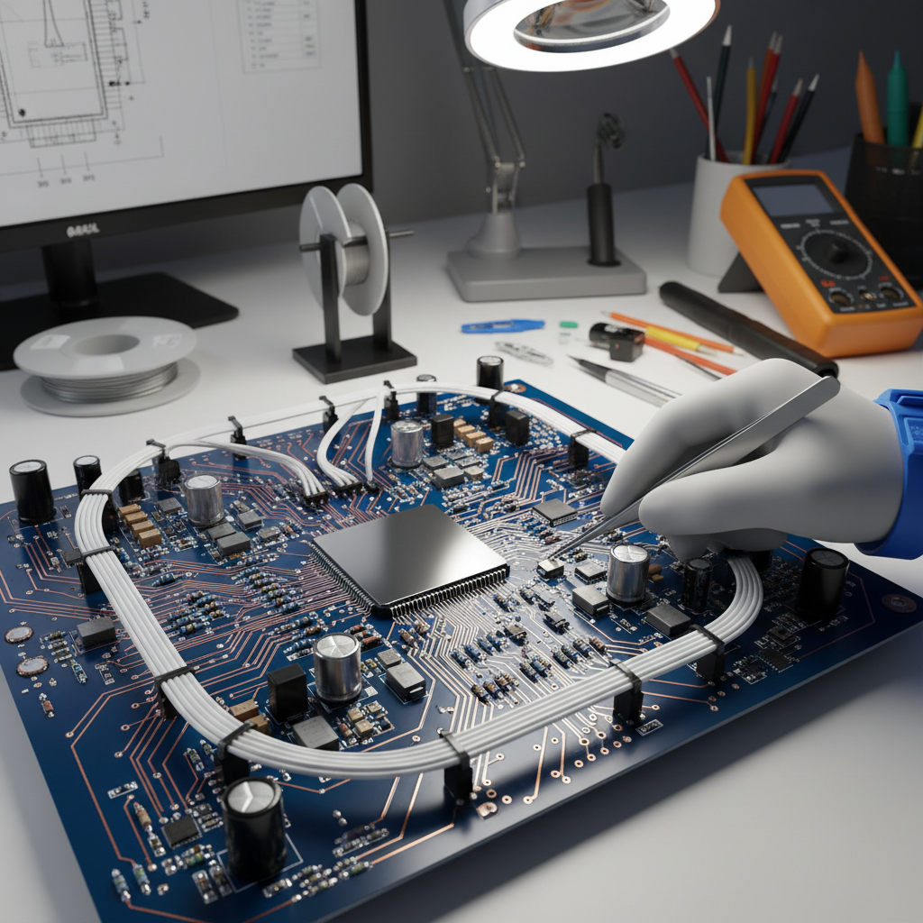
Best Practices for PCB Production and Testing before Mass Production
In the rapidly evolving world of electronics manufacturing,
ensuring the quality and reliability
of printed circuit boards (PCBs) is paramount, especially before scaling to mass production. Implementing
best practices during the production and testing phases can significantly
mitigate risks and enhance product performance. Utilizing automated testing systems
can streamline the detection of defects early in the prototype phase, allowing for adjustments that prevent costly errors later on.
Furthermore, meticulous documentation throughout the design and
production processes aids in maintaining consistency and quality assurance, paving the way for successful mass manufacturing.

Another critical aspect is the adoption of advanced technologies such as
machine learning and data analytics, which are revolutionizing
how manufacturers approach PCB testing. By analyzing historical data, manufacturers can
identify patterns that lead to failures, thus enabling proactive measures in the design phase. Additionally, integrating
feedback loops from testing results can inform iterative improvements, ensuring
that prototypes evolve into robust final products. As we venture into 2025, embracing these trends will empower businesses to not only
stay competitive but also innovate within the
electronics manufacturing landscape.
Common Pitfalls to Avoid During PCB Prototyping and Design Process
When embarking on the PCB prototyping journey, it's crucial to be mindful of common pitfalls that can derail your design and production timeline. A study by the IPC (Institute for Printed Circuits) indicates that nearly 60% of PCB manufacturing issues stem from design errors. This statistic underscores the importance of thorough schematic reviews and adhering to design rule checks (DRC) before finalizing a prototype. Implementing automated DRC tools can significantly reduce human error, allowing designers to focus on innovative aspects of their projects.
Another frequent misstep occurs during the material selection phase. Many designers overlook the impact of substrate materials on final product performance, often choosing based solely on cost rather than suitability. According to a report by PCB Research Group, improper material selection can lead to 30% of a project’s initial budget being spent on rework and redesign. Utilizing materials that match the intended application and environmental conditions is essential for ensuring long-term reliability and functionality, thus streamlining the production process and mitigating unexpected costs associated with revisions. Prioritizing a comprehensive understanding of material properties and benefits can prevent these setbacks and enhance overall efficiency.
How to Create a Perfect PCB Prototype: Tips for Efficient Design and Production - Common Pitfalls to Avoid During PCB Prototyping and Design Process
| Design Aspect |
Best Practice |
Common Pitfall |
| Layer Management |
Use a clear layer stack-up for better manufacturability. |
Overcomplicating the layer arrangement, leading to fabrication errors. |
| Clearances |
Follow the manufacturer’s recommended clearance guidelines. |
Ignoring clearance specifications, causing short circuits or failures. |
| Footprint Design |
Design accurate footprints to match components. |
Using generic footprints that don't accommodate specific parts. |
| Trace Width |
Calculate trace width based on current carrying requirements. |
Underestimating trace width, leading to overheating. |
| Simulation |
Use simulation tools for circuit validation before prototyping. |
Skipping simulation, resulting in unexpected behaviors. |
| Prototype Testing |
Conduct thorough testing on each prototype version. |
Failing to test versions properly, limiting performance understanding. |
| Documentation |
Maintain detailed documentation throughout the design process. |
Neglecting documentation, causing confusion in future revisions. |