How to Efficiently Navigate Prototype PCB Manufacturing Process?
Navigating the prototype PCB manufacturing process can be complex. Understanding each stage is crucial for successful outcomes. Prototype PCB manufacturing involves various steps, including design, fabrication, and assembly. Each step requires meticulous attention to detail and a clear plan.
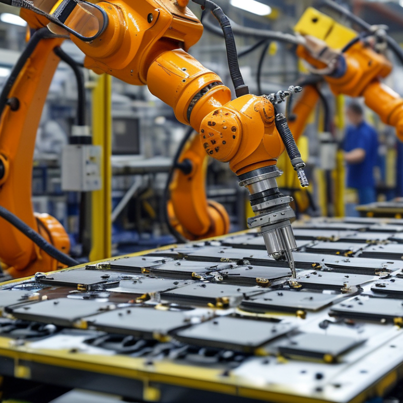
In the design phase, engineers must create precise layouts. Mistakes can lead to significant issues later on. Next, the fabrication process should be chosen carefully. Factors like material type and manufacturing technique are essential. A wrong choice might impact whole project timelines.
Finally, the assembly stage is where everything comes together. Quality control is critical here. Many overlook this part, leading to failed prototypes. Reflecting on these steps is important. Inefficiencies can arise at any point. A thorough understanding of prototype PCB manufacturing can streamline the process and lead to better results.
Understanding the Prototype PCB Manufacturing Process
Navigating the prototype PCB manufacturing process can be challenging. A clear understanding of the steps involved is crucial. Research indicates that the time taken for PCB prototyping can vary significantly. Industry surveys show that up to 40% of projects face delays due to inadequate planning.
Effective communication between designers and manufacturers is vital. Engineers must specify requirements clearly. Data shows that miscommunication leads to 30% of rework in prototype development. This rework can increase costs and extend timelines unexpectedly. Paying attention to detail in the prototyping stage is essential. Small errors can cascade into larger issues later.
Choosing the right materials also plays a critical role. Material selection affects not only functionality but also manufacturability. Reports highlight that 15% of prototypes failed due to inappropriate material choices. This emphasizes the need for thorough research and testing. Engaging with experienced manufacturers can provide insights that help avoid common pitfalls. Engaging in iterative design reviews enhances accuracy, but remember, perfection is a moving target. Testing and learning from mistakes should always be part of the process.
Key Steps in Designing for Prototype PCB Fabrication
Designing a prototype PCB requires meticulous attention to detail. One critical step is
creating a schematic. This represents the circuit's functionality. Industries report that up to
30% of design errors stem from insufficient schematic clarity. Teams must ensure that every
connection is clear and unambiguous. Tools like simulation software can help identify potential issues before production begins.
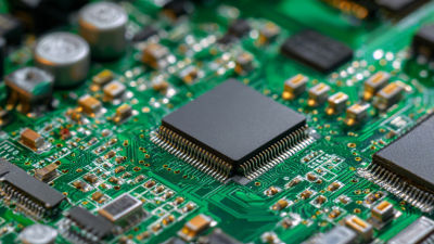
After the schematic is complete, the next step is layout design. This involves placing
components and routing traces. It's recommended that designers consider spacing and trace width meticulously. Inadequate spacing can lead to
electrical interference. According to IPC standards, a 10-mil trace width is often the minimum for reliable
communication. Many designers overlook this, leading to hiccups in functionality. It’s essential to verify the layout with design rule checks.
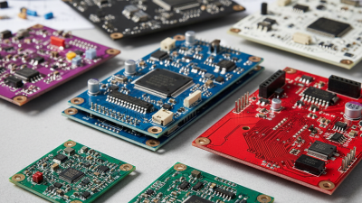
Finally, the fabrication process itself is complex. Choosing the right materials can affect cost and performance. Many companies find that unexpected
changes in specifications can increase lead times by
20%. Attention must be paid to component sourcing and assembly. In some reports, companies experienced
a loss of 15% production time due to miscommunication. Being proactive about
communication and expectations can alleviate these pitfalls.
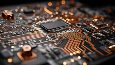
Selecting the Right Materials for Prototype PCBs
Selecting the right materials for prototype PCBs is crucial in the manufacturing process. According to industry reports, nearly 30% of prototyping delays stem from material selection errors. The choice of substrate, copper thickness, and solder mask can significantly affect your PCB's performance and reliability.
For instance, FR-4 is a commonly used material, known for its good balance of cost and performance. Its dielectric constant allows for a stable signal transmission at moderate frequencies. However, the increasing complexity of modern circuits demands materials that can handle higher frequencies.
Materials like Rogers or Polyimide may be necessary for advanced applications. Understanding the electrical, thermal, and mechanical properties of these materials is essential.
It’s important to note that not all materials are suited for every project. The cost of specialized materials can be a barrier, leading teams to compromise on quality. While budget constraints are a reality, it's vital to weigh the long-term implications on performance. In some cases, cheaper materials can result in failure, leading to increased costs and time delays. Testing and validation are necessary steps to ensure that the chosen materials will meet project specifications.
Best Practices for Prototype PCB Testing and Quality Assurance
In the world of prototype PCB manufacturing, testing and quality assurance play a critical role. A recent industry report revealed that around 70% of prototype failures stem from design flaws that went undetected during initial testing phases. Implementing rigorous testing methodologies is essential to avoid costly errors. For instance, visual inspection remains a foundational practice. It allows teams to catch obvious defects, contributing to overall quality assurance efforts.
Functional testing is another vital component. This process evaluates whether the PCB operates as intended under various conditions. Studies indicate that early functional tests can reduce rework by as much as 40%. Incorporating real-time feedback during testing can refine subsequent prototypes. Engineers must remain vigilant, as overlooking minute details in the testing phase can lead to drastic project delays.
Thermal management tests should not be overlooked. They determine how well a PCB dissipates heat under load. With reports showing that thermal issues account for up to 30% of electronic failures, it's evident that rigorous thermal testing can improve reliability. Each testing phase should be treated as a learning opportunity. Documenting and analyzing failures can lead to significant process improvements.
Prototype PCB Testing and Quality Assurance Metrics
Cost Considerations in Prototype PCB Manufacturing
Understanding cost considerations in prototype PCB manufacturing is crucial for optimizing your budget. The initial prototype can be significantly more expensive compared to mass production. This is primarily due to setup costs and smaller order quantities. Each design typically requires specific manufacturing processes and materials, which can vary widely in price.
Choosing the right materials can also affect the overall cost. High-quality substrates and components might enhance performance, but they can add to your expenses. Additionally, intricate designs may require advanced manufacturing techniques, further increasing costs. It’s essential to balance quality and cost to ensure the prototype meets your needs without overspending.
Some companies enter the process with rigid expectations. They might overlook unforeseen expenses like debugging or design adjustments. Prototypes often need fine-tuning, which can lead to unexpected costs. Reflecting on these aspects before committing can significantly impact the project's financial outcome. Understanding potential pitfalls will empower you to allocate resources more wisely for future iterations.
How to Efficiently Navigate Prototype PCB Manufacturing Process? - Cost Considerations in Prototype PCB Manufacturing
| Cost Item |
Description |
Estimated Cost ($) |
Time Frame |
| PCB Material |
Various materials such as FR-4, aluminum, etc. |
50 - 200 |
5-10 Days |
| Fabrication Cost |
Costs associated with manufacturing processes |
100 - 500 |
7-14 Days |
| Assembly Cost |
Cost of placing components on the PCB |
200 - 600 |
5-10 Days |
| Testing |
Final quality assurance and functional testing |
50 - 150 |
3-5 Days |
| Shipping |
Cost to transport the PCBs to the customer |
30 - 100 |
1-7 Days |