2025 How to Explore PCB Ways for Efficient Circuit Design and Production
The efficient design and production of printed circuit boards (PCBs) are crucial in today's fast-paced electronics industry. As technology continues to evolve, exploring innovative PCB ways becomes increasingly important for engineers and manufacturers alike. Noted PCB expert Dr. Emily Carter emphasizes the significance of embracing new methods: "The future of electronic design lies in our ability to adapt and innovate PCB ways that streamline both the creation and functionality of circuits."
With the rise of miniaturization and the demand for more complex devices, understanding and implementing effective PCB design strategies is essential. From optimizing layout and selecting appropriate materials to utilizing advanced manufacturing techniques, the exploration of PCB ways will provide a roadmap for enhancing both efficiency and performance. As we delve into the various approaches to PCB design and production, it is critical to consider both the immediate benefits and the long-term implications of these innovative strategies on the electronics sector.
In this article, we will analyze different PCB ways that can lead to improved circuit design and production processes, setting the stage for breakthroughs that meet the growing needs of modern technology. By leveraging expertise in this field and remaining committed to constant improvement, we can pave the way for a brighter future in electronic manufacturing.

Overview of PCB Basics for Efficient Circuit Design
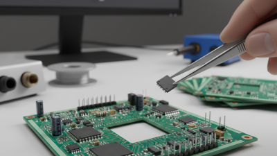
Printed Circuit Boards (PCBs) play a crucial role in modern electronics, serving as the backbone for countless devices. Understanding the fundamentals of PCB design and production is essential for engineers and designers aiming for efficiency. According to a recent study by the IPC (Institute of Printed Circuits), the global PCB market is projected to grow to $78.1 billion by 2025, driven by advancements in technology and increased demand for miniaturized electronic components. This urgency necessitates a focus on streamlined design processes and optimized production methodologies.
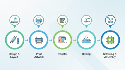
Key principles of efficient PCB design include diligent component placement, trace routing, and thermal management. A well-planned layout can significantly reduce signal loss and electromagnetic interference, enhancing circuit performance. The importance of design software tools cannot be overstated, as they empower designers to simulate and validate their designs before actual production, potentially reducing prototype iterations by up to 40%. Furthermore, employing design for manufacturability (DFM) techniques can lower production costs and lead times while improving yield rates. Industry reports indicate that companies adopting DFM see an average reduction in production costs by 20-30%, underscoring the value of integrating these practices early in the design phase.
By focusing on the basics of PCB design—such as understanding material properties, layer stack-up configurations, and soldering techniques—professionals can enhance both the efficiency and reliability of their circuits. Integrating these design principles alongside innovative manufacturing processes is essential for meeting the growing demands of the electronics industry, paving the way for the advancements expected as we approach 2025.
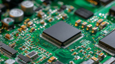
PCB Material Usage in Efficient Circuit Design (2023)
Key Considerations in PCB Materials Selection and Layout
The selection of materials for printed circuit boards (PCBs) plays a pivotal role in ensuring efficient circuit design and production. When choosing PCB materials, several key factors need to be considered, including thermal conductivity, dielectric constant, and mechanical strength. For instance, materials with higher thermal conductivity can help dissipate heat more effectively, enhancing the overall performance and longevity of the circuit. Conversely, a lower dielectric constant can improve signal integrity, making it crucial for high-frequency applications.
Another important consideration in PCB layout is the arrangement of components and traces. A well-thought-out layout minimizes the length of the traces, reducing resistance and potential electromagnetic interference. This not only optimizes the electrical performance but also streamlines the manufacturing process. Additionally, careful positioning of components can aid in effective heat management, further contributing to the durability and efficiency of the PCB. Addressing these material and layout considerations holistically ensures that circuit designs are robust, reliable, and suitable for various applications in an increasingly complex electronics landscape.
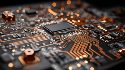
Innovative Techniques for PCB Design Optimization
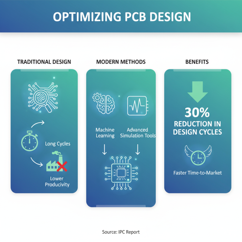
In the fast-evolving landscape of electronics, optimizing PCB (Printed Circuit Board) design is critical for enhancing overall circuit efficiency and production productivity. Innovative techniques such as advanced simulation tools and machine learning algorithms are increasingly being leveraged to streamline the design process. According to a report by IPC, a global trade association for the electronics industry, companies employing these modern methods can achieve up to 30% reduction in design cycles, significantly accelerating time-to-market for new products.
Furthermore, adopting design for manufacturability (DFM) principles is proving to be a game changer in PCB optimization. By integrating feedback from manufacturing early in the design phase, engineers can identify potential issues that may affect production efficiency. Studies have shown that implementing DFM strategies can reduce production costs by as much as 20%, while simultaneously minimizing the likelihood of design errors. As the industry moves toward more complex circuit designs, these innovative techniques will become essential for staying competitive and ensuring the reliability of electronic products.
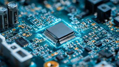
Advancements in PCB Manufacturing Technologies
Recent advancements in PCB manufacturing technologies have revolutionized the landscape of circuit design and production. One of the most significant developments is the introduction of additive manufacturing techniques, which allows for the creation of PCBs with intricate geometries and features that were previously challenging to achieve. This method not only enhances design flexibility but also reduces material waste, leading to more sustainable production processes. By utilizing advanced printing technologies, manufacturers can produce high-density interconnects and complex layer structures that cater to the growing demands of modern electronics.
Furthermore, the integration of automation and AI-driven processes in PCB manufacturing has significantly improved efficiency and precision. Automated inspection systems employ sophisticated algorithms to detect defects early in the production cycle, ensuring higher quality and reliability in finished products. Additionally, AI can optimize the PCB design process by simulating performance under various conditions, allowing designers to make data-driven decisions. These technologies collectively streamline production workflows, reduce lead times, and enable manufacturers to respond more swiftly to market needs, thus setting the stage for future innovations in circuit design.
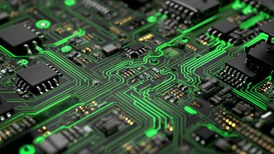
Best Practices for Testing and Quality Assurance in PCB Production
Ensuring high-quality production standards in PCB manufacturing is crucial for optimal performance and reliability in electronic devices. According to a report by IPC, over 30% of PCB failures are attributed to manufacturing defects, highlighting the importance of robust testing and quality assurance practices. Integrating automated optical inspection (AOI) into the production line can significantly reduce such defects. AOI systems use advanced imaging technologies to detect abnormalities in the PCB, ensuring that any issues are identified before further processing. By adopting AOI, manufacturers can achieve defect detection rates exceeding 98%, leading to lower rework costs and increased production efficiency.
Moreover, implementing end-of-line testing methods, such as in-circuit testing (ICT) and functional testing, further enhances quality assurance. A study from Electronics Protection noted that devices subjected to rigorous testing showed a 40% decrease in field failure rates. These tests verify the functionality and electrical performance of the boards, ensuring that they meet specified design criteria. In addition, a proactive feedback loop between the testing phase and design engineering can lead to continuous improvement in manufacturing processes, fostering a culture of quality that is essential for long-term success in PCB production. By prioritizing these best practices, companies can not only enhance product reliability but also respond effectively to the growing demands of modern circuit design.