How to Make PCB at Home Step by Step Guide for Beginners
In recent years, the demand for printed circuit boards (PCBs) has seen significant growth, fueled by advancements in technology and increased adoption of electronics across various industries. According to a report by IPC, the global PCB market is projected to reach approximately $82 billion by 2024, reflecting a compound annual growth rate (CAGR) of around 4.5% from 2019 to 2024. This growth underscores the increasing need for individuals and small businesses to learn how to make PCBs at home, enabling innovation, prototyping, and customization in electronic projects.
For beginners, the process of making PCBs may seem daunting, yet it can be both educational and rewarding. With the right guidance and tools, anyone can embark on this journey and develop their skills in electronics. DIY PCB fabrication not only helps in the cost-cutting of small projects but also boosts creativity by allowing hobbyists to bring their designs to life without relying solely on external manufacturers. As more enthusiasts explore the potential of home PCB production, understanding the step-by-step process becomes essential for harnessing the capabilities of modern electronics effectively. In this guide, we will break down the process of making PCBs at home, ensuring newcomers find it accessible and manageable.
Understanding PCB Basics and Components
Printed Circuit Boards (PCBs) are essential components in most electronic devices, providing a platform for circuit connections. Understanding the fundamental aspects of PCBs is crucial for anyone looking to create their own circuits at home. At its core, a PCB consists of a substrate, usually made from materials such as fiberglass or epoxy resin, which supports the arrangement of electronic components like resistors, capacitors, and integrated circuits. These components are connected with conductive pathways, typically made from copper, that facilitate the flow of electricity.
When embarking on PCB design, it is important to familiarize oneself with various components and their functions. Resistors, for instance, limit the current flowing through a circuit, while capacitors store and release energy as needed. Diodes, on the other hand, allow current to flow in one direction only, providing essential functionality in many circuits. Understanding the role of these components, along with others like transistors and inductors, is vital for designing effective and efficient PCBs. As beginners delve into the world of PCB creation, grasping these basic principles will lay the foundation for more complex projects in electronics.
Necessary Tools and Materials for PCB Making
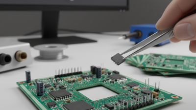
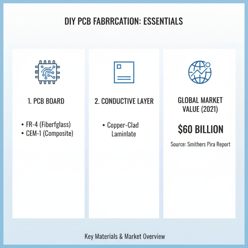
To begin the process of making a PCB at home, you’ll need to gather several essential tools and materials. At the core of PCB fabrication is the PCB board itself, typically made from materials like FR-4 or CEM-1. These substrates provide the necessary insulation and mechanical properties. Additionally, you’ll require copper-clad laminate, which serves as the conductive layer for your circuits. According to a report by Smithers Pira, the global market for PCBs was valued at approximately $60 billion in 2021, indicating just how integral these components are to electronics manufacturing.
In terms of tools, a strong UV light source or an exposure unit is necessary for transferring your PCB design onto the copper surface. A photoresist film is another critical component that allows you to create precise circuit patterns when exposed to light. A quality etching solution, typically ferric chloride, is essential for removing unwanted copper after developing your circuit. Furthermore, you will need a soldering iron to connect electronic components to the PCB once it's ready. It’s important to ensure that you have adequate ventilation and safety equipment, as some of these materials can be hazardous. A study by IPC International indicates that around 70% of PCB manufacturers consider material quality and supplier reliability pivotal, which highlights the importance of sourcing reputable materials for personal projects as well.
Step-by-Step Process for Designing Your PCB Layout
Designing a PCB layout is a critical step in the process of creating your own printed circuit boards at home. As the demand for custom electronic devices increases, understanding how to effectively design a PCB becomes essential for DIY electronics enthusiasts and makers. According to a report by IPC, the global PCB market is expected to reach $84.25 billion by 2024, highlighting the growing significance of PCB design and manufacturing skills in the electronics industry.
To start, utilize PCB design software that allows you to create schematics easily. Begin by importing your circuit diagram and then lay out the components on the PCB surface. Pay close attention to component placement; grouping related components can minimize routing complexity and enhance the signal integrity. According to a survey from Altium, nearly 60% of design errors stem from poor layout practices. To avoid such pitfalls, establish clear design rules, such as maintaining appropriate trace widths and clearance distances, guided by industry-specific standards like IPC-2221.
Once the layout is established, use the routing tools to connect the components efficiently. Employing techniques such as differential pairs for critical signals can significantly reduce electromagnetic interference (EMI). A well-optimized layout not only improves performance but also reduces manufacturing costs; as noted by a recent study, well-designed PCBs can lead to a 30% reduction in production costs. By following a systematic approach to PCB layout design, beginners can create effective and reliable printed circuit boards tailored to their specific needs.
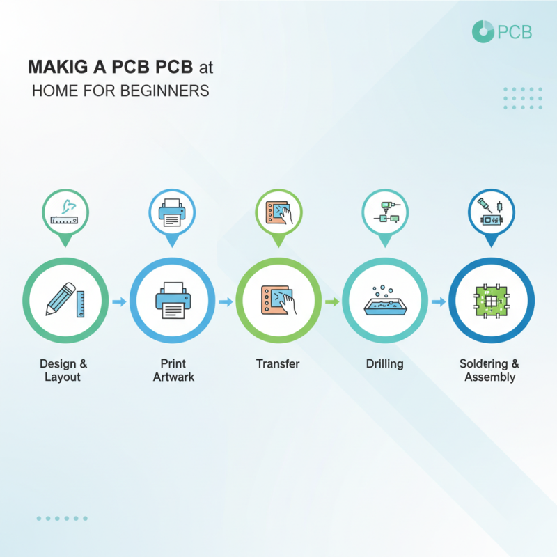
How to Make PCB at Home Step by Step Guide for Beginners - Step-by-Step Process for Designing Your PCB Layout
| Step |
Description |
Materials Needed |
Estimated Time |
| 1 |
Design your PCB layout using software. |
PCB design software (e.g., KiCAD, Eagle) |
1-2 hours |
| 2 |
Print the design onto a specific photo paper. |
Laser printer, photo paper |
30 minutes |
| 3 |
Transfer the printed design to the copper-clad board using heat. |
Copper-clad board, iron |
15 minutes |
| 4 |
Etch the PCB to remove unneeded copper. |
Etching solution (e.g., ferric chloride) |
30 minutes |
| 5 |
Drill holes for components. |
Drill, drill bits |
20 minutes |
| 6 |
Solder components onto the board. |
Soldering iron, solder, components |
1-2 hours |
| 7 |
Test the completed PCB for functionality. |
Multimeter |
30 minutes |
Techniques for Transferring PCB Design to Material
When transferring your PCB design to the material, several techniques can be utilized to achieve a high-quality result. One of the most popular methods is the toner transfer technique. This involves printing your design onto glossy paper using a laser printer and then transferring the toner onto the copper-clad board using heat. After aligning the printed paper with the board, place it under a hot iron to melt the toner into the copper surface, creating a blueprint for etching.
Another method is the use of photoresist. This process entails applying a photoresist film on your copper board and exposing it to UV light through your design transparency. The areas exposed will harden, while the unexposed regions can be washed away, leaving a clear pattern for copper etching. This method is known for providing better resolution and detail in your designs, which is especially beneficial for intricate circuits.
Tips: Always ensure your workspace is clean and your materials are organized. A messy environment can lead to mistakes in alignment and positioning. It is also advisable to practice the toner transfer technique on scrap materials before moving on to your actual PCB design. Lastly, using high-quality glossy paper can significantly improve the transfer quality, resulting in better-defined patterns on your board.
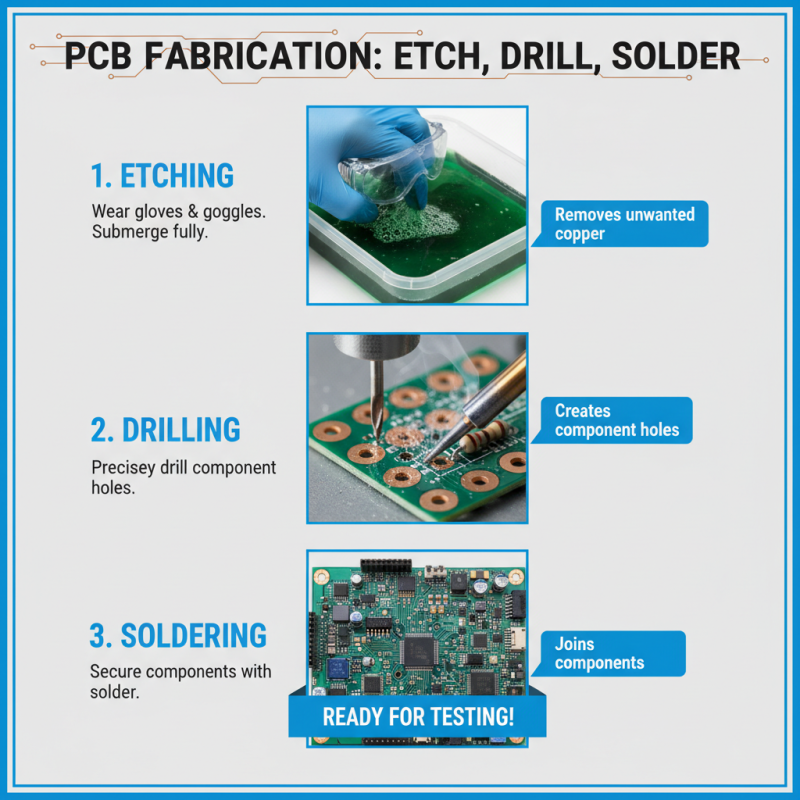
Finishing Touches: Etching, Drilling, and Soldering Your PCB
After you have designed your PCB and printed the layout, the next crucial steps involve etching, drilling, and soldering. Etching is a process that removes unwanted copper from the board using a chemical solution. It's essential to prepare your workspace by wearing protective gloves and goggles, as the chemicals involved can be hazardous. For effective etching, ensure that the exposed copper areas are well-defined and that the board is fully submerged in the etchant solution for the required time.
Tips: Always agitate the etchant solution gently to enhance the etching process. If you're unsure about the timing, check the board frequently to prevent over-etching, which can damage the circuitry. Additionally, it can be helpful to mark the time on a timer to keep track without constantly checking.
Once the etching is complete, the next step is drilling the holes for your components. Use a precision drill and ensure you're drilling at the correct size for your specific components. It's advisable to practice on a scrap piece of material to get a feel for the process if you're a beginner.
Tips: Keep the drill speed moderate to avoid damaging the board, and always drill from the copper side to minimize delamination. Lastly, when moving on to soldering, make sure to use the correct solder wire and a good quality soldering iron. Pre-tinning your components can also help improve joint quality.