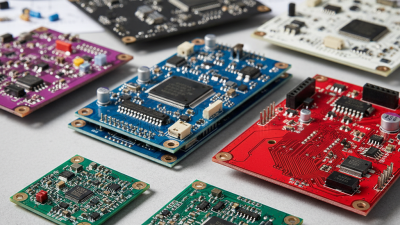
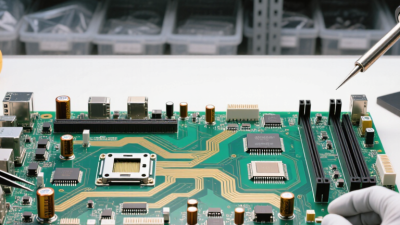
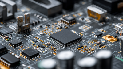
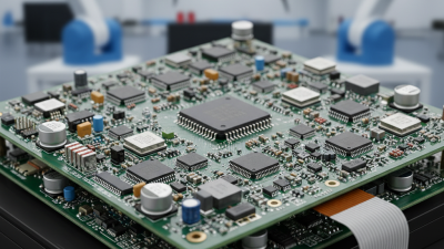
What Is PCB and Assembly for Global Buyers? The question sounds simple, but it covers two connected manufacturing decisions. A printed circuit board, or PCB, provides the electrical platform. Assembly adds components through processes such as solder paste printing, pick-and-place placement, reflow soldering, and inspection. Together, pcb and assembly transform design files into a testable electronic product.
The commercial importance is measurable. The World Semiconductor Trade Statistics (WSTS) Autumn 2024 Forecast projected global semiconductor sales to approach 700 billion U.S. dollars in 2025. More components create greater demand for reliable board manufacturing and assembly capacity. IPC’s electronics manufacturing standards, including IPC-A-610 and J-STD-001, also show why workmanship cannot depend on appearance alone. Solder joints, cleanliness, traceability, and process control matter.
Global buyers must examine more than unit price. A supplier should explain its material grade, layer construction, copper thickness, component sourcing, inspection coverage, and production controls. A bare board may look perfect under ordinary light. It can still fail during thermal cycling or vibration testing. That detail is often missed.
The phrase “pcb and assembly” is sometimes used too loosely. It may describe fabrication only, or a complete turnkey service. Buyers should clarify the scope before requesting quotations. Gerber files, bill of materials, pick-and-place data, drawings, and approved alternates should match. Small inconsistencies can delay production.
This article introduces the technical language, purchasing checkpoints, quality expectations, and supply-chain risks that global buyers should understand. No supplier is automatically reliable. Evidence, repeatable processes, and transparent communication provide stronger proof.
A printed circuit board, or PCB, is the rigid or flexible platform that connects electronic components. Copper traces carry signals and power across its surface. A bare PCB has no installed components. It may include drilled vias, solder pads, controlled-impedance lines, and several laminated layers.
A four-layer board is common in industrial controllers and communication equipment. It offers better routing and grounding than a simple two-layer design.
PCB assembly, often called PCBA, adds components to that board. The process may include solder paste printing, pick-and-place mounting, reflow soldering, through-hole insertion, and inspection.
Optical inspection checks solder joints and component positions. X-ray inspection can reveal hidden defects under packaged devices.
According to Mordor Intelligence, the global PCB market is valued above 80 billion US dollars in the mid-2020s. That scale reflects demand for compact, reliable electronics, not just higher production volume. Small design errors still create expensive delays.
For global buyers, the difference matters during quotation and quality review. A PCB supplier may deliver bare boards only. An assembly supplier may source components, mount them, program devices, and complete functional testing.
IPC market research has consistently identified material costs, lead times, and supply continuity as major electronics-industry concerns.
Buyers should therefore confirm layer count, copper thickness, surface finish, component sourcing, inspection coverage, and acceptance standards.
I would not treat “assembled” as proof of quality. Test records, traceability, and clear revision control deserve closer attention. The drawing may look finished, yet one missing tolerance can change the entire production result.
A printed circuit board, or PCB, provides the electrical and mechanical foundation for an electronic product. Engineers begin with a schematic, then convert it into a controlled layout. They position components, route copper traces, define impedance, and add mounting holes. Design teams also check heat, signal timing, creepage distance, and manufacturing limits. Small errors matter. A misplaced via can reduce yield or create difficult repairs.
Manufacturing usually starts with copper-clad laminate. Computer-controlled machines drill holes, form circuit patterns, plate copper, and apply solder mask. Automated optical inspection checks image defects, while electrical testing confirms circuit continuity and isolation. Assembly follows with solder paste printing, component placement, reflow, and final inspection. IPC standards guide many acceptance and workmanship decisions. However, standards do not replace engineering judgment.
Market data shows why design discipline matters. Prismark estimated global PCB sales at approximately 69 billion US dollars in 2023, after a significant market decline. Its industry forecasts also highlight continued demand for high-density interconnects and advanced substrates. IPC’s International Technology Roadmap points toward finer lines, higher layer counts, and stronger thermal control. These trends increase capability, but also raise fabrication risk. Global buyers should request stack-up drawings, material specifications, test records, and yield data before production. A design that works in simulation may still fail during drilling, plating, or thermal cycling. That gap deserves honest review.
What Happens During the PCB Assembly Process?
What happens after a PCB design leaves engineering? PCB assembly turns bare laminate into a tested electronic unit. Operators begin by checking components, drawings, and the bill of materials. Incoming inspection catches wrong values, damaged leads, and moisture-sensitive parts. That small pause matters. Global semiconductor sales reached $626.9 billion in 2024, according to the December 2024 WSTS market forecast. Rising component variety makes traceability less optional.
Next, a stencil printer deposits solder paste onto copper pads. A 2D paste inspection system measures coverage, height, and alignment. Pick-and-place machines position resistors, processors, connectors, and tiny passive parts. The board then passes through a reflow oven, where controlled heat melts the paste. Profiles must match the solder alloy and component limits. Excess heat can cause warping or hidden joint damage. Through-hole parts may receive selective soldering afterward. Defects hide well.
Inspection continues with automated optical inspection, electrical tests, and functional checks. IPC acceptance criteria are commonly used to judge solder joints, spacing, and component placement. X-ray inspection can reveal voids under bottom-terminated components. Each failure should lead to a documented correction, not quiet rework. A rushed pilot run may pass while exposing weak process control later. Buyers should request defect records, test coverage, traceability, and sample approval before volume production. Ask for evidence.
| Process Stage | Main Purpose | Typical Inputs | Key Controls and Equipment | Expected Output | Global Buyer Checkpoints | Typical Timing |
|---|---|---|---|---|---|---|
| 1. Engineering Review and DFM | Confirm that the PCB design can be manufactured and assembled consistently. | Gerber or ODB++ files, drill files, schematic, bill of materials, pick-and-place data, assembly drawings and test requirements. | Design-for-manufacturing review, design-for-assembly review, component availability check and engineering change control. | Validated manufacturing data, clarified tolerances and an approved production package. | Check revision control, component substitutions, package compatibility, polarity information and acceptance criteria. | Before quotation or production |
| 2. Bare PCB Fabrication | Produce the unassembled printed circuit board that provides electrical connections and mechanical support. | Core and prepreg materials, copper foil, solder mask, legend ink and specified surface finish. | Layer registration, controlled impedance where required, copper thickness, hole quality, solder mask alignment and surface-finish inspection. | Tested bare PCBs ready for component assembly. | Verify layer count, board thickness, copper weight, finish, material requirements, panelization and electrical test coverage. | Often several working days |
| 3. Incoming Material Inspection | Confirm that boards and components meet the approved production requirements before assembly. | Bare PCBs, integrated circuits, passive components, connectors, mechanical parts and moisture-sensitive devices. | Part-number and quantity verification, lot traceability, packaging inspection, date-code review where applicable and moisture-control procedures. | Accepted materials, quarantined nonconforming materials or an approved deviation record. | Request component traceability, counterfeit-prevention controls, shelf-life rules and a documented nonconformance process. | Before line setup |
| 4. Solder Paste Printing | Apply a controlled amount of solder paste to the PCB pads for surface-mount components. | PCB panels, solder paste, stencil and printer setup data. | Stencil aperture design, alignment, paste storage and thawing, print pressure, speed, separation and solder paste inspection. | PCBs with accurately deposited solder paste. | Review paste type, alloy, stencil thickness, fine-pitch capability and inspection records for print volume and alignment. | Minutes per panel |
| 5. Pick-and-Place Assembly | Place surface-mount components onto the solder-pasted PCB in the correct position and orientation. | Printed circuit boards, component reels or trays, feeder setup, placement files and component library data. | Machine vision, feeder verification, component recognition, placement accuracy and polarity control. | Populated PCBs with components held in solder paste. | Confirm component orientation, alternate part approval, feeder verification, placement accuracy and traceability by board or lot. | Seconds to minutes per panel |
| 6. Reflow Soldering | Heat the assembled PCB according to a controlled thermal profile so the solder forms reliable joints. | Paste-printed and populated PCB panels. | Preheat, soak, reflow and cooling zones; profile measurement; conveyor speed; peak temperature and time above liquidus. | Surface-mount components soldered to the PCB. | Request the approved thermal profile, profile verification method, board-specific limits and handling rules for heat-sensitive parts. | Several minutes per batch or panel |
| 7. Through-Hole Component Insertion | Install components whose leads pass through drilled holes in the PCB. | Through-hole components, PCBs and insertion instructions. | Manual or automated insertion, lead forming, polarity verification, insertion-depth checks and component presence checks. | PCB assemblies with through-hole components installed. | Confirm lead-forming requirements, connector alignment, keep-out areas, mechanical fit and approved soldering method. | Depends on component count |
| 8. Wave, Selective or Hand Soldering | Create solder joints for through-hole components and any areas not suitable for reflow. | Inserted components, soldering materials, fixtures and thermal-profile requirements. | Flux application, preheat, solder temperature, contact time, nozzle selection, operator qualification and joint inspection. | Through-hole solder joints completed with acceptable fillets and no harmful bridges. | Specify solder alloy, flux requirements, cleanliness limits, solder-joint criteria and rework authorization. | Minutes per batch or assembly |
| 9. Automated Optical Inspection | Detect visible assembly defects before functional testing. | Assembled PCBs, reference images, component library data and inspection rules. | Camera-based inspection for missing, misplaced or incorrectly oriented components, solder bridges, insufficient solder and tombstoning. | Inspection results, defect images and repaired or released assemblies. | Ask for defect classification, false-call handling, inspection coverage and records linked to the assembly revision. | Seconds per board |
| 10. X-Ray Inspection | Inspect hidden solder joints and internal connections that cannot be evaluated visually. | Assemblies containing bottom-terminated components, area-array packages or other concealed joints. | Two-dimensional or three-dimensional X-ray imaging, void evaluation and solder-joint analysis. | Evidence of acceptable hidden joints or a documented corrective-action requirement. | Determine whether X-ray is required for the package mix, thermal pads, void criteria and sampling plan. | As required by design |
| 11. Cleaning and Visual Inspection | Remove process residues when required and verify general assembly workmanship. | Assembled PCBs, approved cleaning materials and inspection criteria. | Cleaning method compatibility, ionic cleanliness testing where specified, magnification and workmanship inspection. | Clean, visually acceptable assemblies with documented inspection status. | Define no-clean or cleaned-process requirements, residue limits, conformal-coating compatibility and cosmetic standards. | Minutes per assembly |
| 12. Programming and Functional Test | Confirm that the assembly powers up, communicates and performs its intended electrical functions. | Test fixtures, firmware, programming files, test procedures and approved product limits. | In-circuit test where applicable, flying-probe test, boundary-scan test, programming verification and functional test equipment. | Pass or fail results, programmed assemblies and test records. | Supply test specifications, fixture ownership terms, firmware revision control, failure-analysis rules and retest limits. | Seconds to several minutes per unit |
| 13. Rework and Corrective Action | Repair nonconforming assemblies and prevent recurring process defects. | Defect reports, replacement components, approved rework instructions and root-cause data. | Controlled soldering and rework tools, component replacement records, repair inspection and corrective-action review. | Repaired assemblies or documented scrap and process-improvement actions. | Require rework authorization, repair traceability, limits on repeated rework and evidence of root-cause closure. | Varies by defect |
| 14. Final Inspection and Documentation | Verify that the completed order conforms to specifications before shipment. | Finished assemblies, purchase requirements, inspection records and approved drawings. | Final visual inspection, dimensional checks, quantity verification, label review and document-package review. | Released assemblies with inspection and test documentation. | Confirm certificate requirements, inspection reports, test logs, material declarations, packaging instructions and change history. | Before shipment |
| 15. Packaging and International Shipment | Protect assemblies from electrostatic discharge, moisture, shock and handling damage during global transportation. | Finished PCBs, moisture-barrier packaging, desiccant, labels, protective materials and shipping documents. | Electrostatic-discharge protection, moisture control, cushioning, carton identification and export documentation. | Shipment-ready assemblies with traceable packaging and logistics records. | Specify packaging quantity, ESD requirements, moisture sensitivity, carton labels, delivery terms and customs documentation. | After final release |

For global buyers, PCB specifications begin with the board’s electrical and mechanical requirements. Layer count, material grade, copper thickness, and controlled impedance affect performance and pricing. A four-layer board may look sufficient, yet high-speed signals can require tighter stack-up control. Confirm dielectric thickness, trace width, spacing, and impedance tolerance before ordering. Small differences matter.
Assembly specifications deserve equal attention. Provide the component list, placement files, polarity details, and approved substitutions. State soldering requirements, inspection standards, and acceptable defect limits. Lead-free processing may be necessary for certain markets. Testing should include automated optical inspection, electrical testing, and functional checks when applicable. Clear records improve reliability.
In practical production reviews, packaging is often underestimated. Moisture-sensitive components need sealed bags, humidity indicators, and controlled storage instructions. Ask for lot traceability, inspection reports, and sample approval procedures. Confirm whether the supplier can meet required certifications and regional chemical restrictions. Delivery terms, carton labels, and export documents also need precise wording. A neat drawing can still hide risk. I have seen projects delayed by one missing tolerance. Specifications should be reviewed by engineering, purchasing, and quality teams together, even when that feels slower. That extra discussion may prevent expensive rework.
What Is PCB and Assembly for Global Buyers?
A printed circuit board, or PCB, provides the electrical paths connecting components. Assembly adds chips, connectors, solder, inspection, and functional testing. For global buyers, the difficult decision is rarely the lowest unit price. It is supplier control. McKinsey’s 2020 Global Supply Chain Survey reported that 93% of supply-chain leaders planned to increase resilience after major disruptions. That finding still matters when one missing component can stop a complete production order.
Evaluate suppliers through evidence, not polished presentations. Request recent audit records, process capability data, traceability samples, and first-article inspection reports. Confirm their experience with your board’s layer count, material type, component package, and expected monthly volume. IPC standards can guide acceptance criteria for soldering and workmanship. Ask how they manage counterfeit-risk screening and approved substitutions. Then test communication: send a drawing revision and measure the response. Slow answers are data.
Order management needs a controlled document trail. Freeze the bill of materials, revision number, delivery terms, and inspection plan before payment milestones. Use a pilot batch first. Track component availability weekly, especially for long-lead semiconductors. The World Bank’s Commodity Markets Outlook has repeatedly shown how sharply material prices can move during supply disruptions. However, buyers sometimes overvalue dashboards and undervalue shop-floor verification. A supplier may report 98% on-time delivery, yet hide repeated partial shipments. I would inspect packing photos, serial records, and actual arrival dates. Numbers need context.
A practical weighting model for comparing PCB assembly suppliers and managing international orders. Buyers can score each supplier against these criteria before placing prototype or production orders.
Quality and delivery reliability receive the highest weights because defects, rework, and late shipments can create greater total costs than the quoted unit price. The model also highlights traceability, technical support, capacity, and commercial terms when evaluating cross-border PCB assembly orders.
The percentages represent a neutral procurement scorecard framework and are not supplier-specific performance results.