What is PCB and Assembly Process in Electronics?
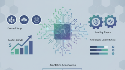
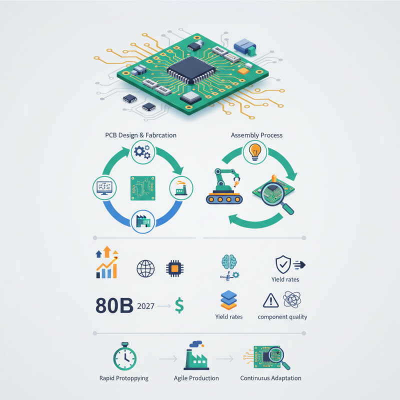
The PCB and assembly process stands as a pivotal component in the electronics industry. As the backbone of modern devices, printed circuit boards (PCBs) enable complex functionalities. According to a recent report by Allied Market Research, the global PCB market is projected to exceed $80 billion by 2027. This growth reflects the increasing demand for electronic devices across various sectors.
Dr. Emily Watson, a leading expert in electronics manufacturing, emphasizes the importance of this process: “Efficient PCB and assembly techniques are essential for innovation.” Her insight highlights both the potential and challenges within the industry. Despite advances, issues like yield rates and component quality remain critical concerns. Manufacturers often strive for perfection but must confront varying standards and regulations.
In an era where rapid prototyping and agile production are paramount, the PCB and assembly process must evolve. Companies face obstacles, such as maintaining quality while scaling operations. The complexity of modern electronics requires continuous adaptation and improvement. Without proper focus on these elements, the industry risks stagnation.
What is a PCB: Definition and Key Components in Electronics
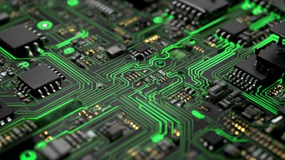
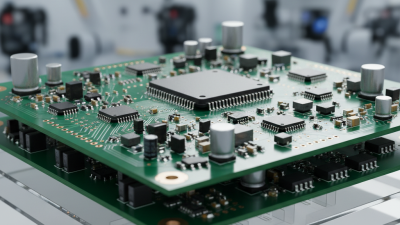
A PCB, or printed circuit board, plays a crucial role in electronics. It serves as a foundation for connecting electronic components. Typically made of insulating material, it features conductive pathways for electric currents. These pathways are often made from copper.
Key components of a PCB include traces, pads, and vias. Traces are the paths through which electricity flows. Pads function as connection points for components, such as resistors or capacitors. Vias are small holes that allow connections between different layers. Sometimes, the layout may be complex. This complexity can lead to manufacturing errors.
Designing a PCB requires attention to detail. Mistakes can cause electrical failures. It's essential to verify every connection and component placement. Yet, even with thorough checks, issues may still arise during assembly. This highlights the challenging nature of PCB design.
The Role of PCB in Electronic Circuit Functionality and Design
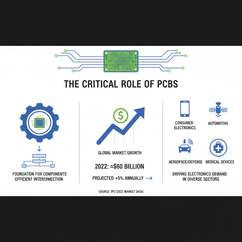
Printed Circuit Boards (PCBs) play a pivotal role in electronic circuit functionality. They provide the foundation for electronic components to connect and interact efficiently. According to IPC, the global PCB market reached approximately $60 billion in 2022 and is projected to grow by 5% annually. This growth signifies the increasing demand for electronics in various sectors.
The design of PCBs directly impacts the performance of electronic devices. They must carefully accommodate different components, such as resistors, capacitors, and chips. A study by Research and Markets indicates that poor PCB layout can lead to signal integrity issues, affecting overall circuit functionality. Designers face challenges like minimizing electromagnetic interference and ensuring optimal heat dissipation. Each decision, from trace width to layer count, influences performance.
Moreover, there are imperfections in the PCB manufacturing process. Inaccurate placements or faulty connections can occur, leading to longer production times. Industry reports show that nearly 10% of PCBs face assembly defects. These recurring issues prompt designers to continuously refine their processes. They must weigh the trade-offs between cost, quality, and manufacturability in an increasingly competitive market.
Overview of the PCB Manufacturing Process: Steps and Technologies
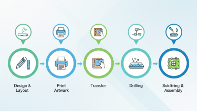
The PCB manufacturing process involves several steps that transform raw materials into functional circuitry. The journey begins with the design phase, where engineers create layouts using specialized software. This layout defines the electronic pathways and component placements. Next, the design is printed onto a copper-clad board. This step requires precision. Any error can compromise the entire project.
Once the design is transferred, the board undergoes etching. Unwanted copper is removed, revealing the circuit pattern. This stage is crucial. A slight mishap can lead to short circuits. After etching, it’s time to drill holes for components. Again, accuracy is essential. Drilling too far off can lead to assembly issues later.
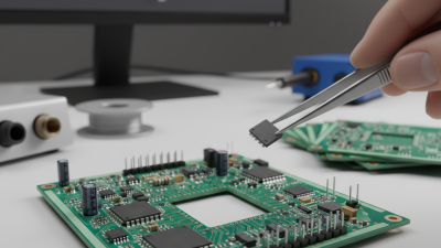
Following the drilling, the boards are cleaned and coated for protection. This process is sometimes rushed, leading to issues. Some manufacturers overlook the importance of quality checks. This can create bigger problems in assembly. After coating, the components are placed and soldered onto the board. Each of these steps is vital. Omissions can result in a product that fails to perform its intended function.
Assembly Process: Techniques for Mounting Components on PCB
The assembly process of a printed circuit board (PCB) involves several critical techniques for mounting components. Surface mount technology (SMT) is prevalent in the industry due to its efficiency. According to a 2022 report from IPC, around 75% of PCBs are assembled using SMT. This method allows for higher component density, which is essential in modern electronics.
Another technique is through-hole mounting. While not as common for high-density applications, it offers robust connections, especially for larger components. This method remains relevant in sectors such as automotive and industrial electronics. Data shows that approximately 25% of assemblies still utilize through-hole techniques. Challenges arise with rework processes, often leading to increased costs and time delays.
Moreover, the industry's shift towards automation makes solder paste printing crucial. Robotic systems are becoming the norm, yet mistakes can occur, such as misalignment or insufficient paste application. How to minimize these errors continues to be a vital question among engineers. The quest for perfection in assembly leads to ongoing evaluations of both manual and automated techniques. Balancing cost and precision remains a continuous struggle.
Quality Control in PCB Assembly: Standards and Testing Metrics
Quality control is a crucial part of the PCB assembly process. It ensures the reliability and functionality of electronic devices. Common standards include IPC-A-610 and IPC-2221. These guidelines help companies maintain consistency. They outline acceptable workmanship, materials, and testing methods. Adhering to these standards is not just about passing inspections. It’s about building trust with customers.
Testing metrics play a significant role in quality assessment. Visual inspections are often the first step. However, they don’t catch every issue. Automated optical inspection (AOI) provides a more thorough review. X-ray inspection is also valuable, especially for hidden solder joints. These methods can reveal faults like misalignment or insufficient solder. Yet, even advanced techniques may miss some defects. Continuous improvement is essential in this ever-evolving field.
Companies sometimes overlook the human element. Training can be inconsistent. Employees may not always follow the established protocols. Regular training sessions can help counteract this. Balancing automation with human skill is key. Effective communication within teams is also vital. All these factors contribute to the overall quality of PCB assembly.
What is PCB and Assembly Process in Electronics? - Quality Control in PCB Assembly: Standards and Testing Metrics
| Quality Control Metrics |
Standard |
Testing Method |
Acceptable Range |
| Visual Inspection |
IPC-A-610 |
Manual Inspection |
100% inspection |
| Electrical Testing |
IPC-6012 |
In-Circuit Test (ICT) |
Pass/Fail |
| Functional Testing |
ISO 9001 |
Functional Test Setup |
Defined functional limits |
| Thermal Cycling Test |
MIL-STD-202 |
Thermal Shock Test |
-55°C to +125°C |
| X-Ray Inspection |
IPC-TO-709 |
Non-destructive Testing |
Critical component alignment |