Top PCB Board Fabrication Methods for Global Buyers?
In the dynamic world of electronics, the demand for reliable and high-quality PCB board fabrication continues to rise. Leading industry expert Dr. Emily Chen once stated, “The quality of PCB board fabrication can significantly influence the overall performance of electronic devices.” This highlights the critical role that fabrication methods play in ensuring product reliability.
As global buyers seek the best options for PCB board fabrication, understanding the various methods available is essential. Techniques like subtractive, additive, and hybrid fabrication each offer unique advantages. For instance, subtractive methods are widely used for their precision, while additive methods are gaining traction for flexibility and reduced waste. However, the choice may vary based on specific project needs and challenges.
Despite advancements in technology, the PCB board fabrication process is not without flaws. Issues such as material quality and design limitations can arise. Buyers must critically assess their options and remain informed about potential pitfalls. By doing so, they can make better choices that align with their project goals.
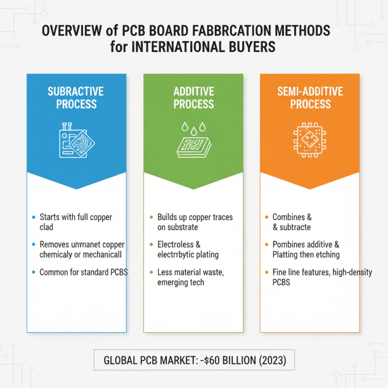
Overview of PCB Board Fabrication Methods for International Buyers
When considering PCB board fabrication methods, international buyers must evaluate several key techniques. Among the most common methods are subtractive, additive, and semi-additive processes. According to industry reports, the global PCB market has reached approximately $60 billion in 2023, highlighting the importance of understanding these fabrication techniques.
Subtractive manufacturing removes material from a pre-existing substrate. This method is cost-effective for larger batches. Additive techniques, on the other hand, build layers up. This is particularly useful for producing high-density interconnects designed for compact electronics. One challenge to note is that while additive methods reduce waste, mastering them requires advanced technology and skilled personnel.
The semi-additive process combines elements of both methods. It is gaining popularity for its ability to produce fine lines and spaces. However, it also has a steeper learning curve. A recent study indicated that nearly 40% of consumers are looking for sustainable alternatives in PCB production. This reflects a growing need for fabricators to adapt. Overall, understanding these methods greatly influences sourcing decisions for global buyers navigating the complexities of PCB manufacturing.
Key Factors Influencing PCB Fabrication Technique Choices
When selecting PCB fabrication techniques, several key factors come into play. These include
project requirements,
material types, and production volume. According to industry reports, choosing the right method can reduce costs by up to 30%.
For instance, traditional subtractive methods like etching are commonly used for simple designs. However, these can be less efficient for complex circuits.
Another important consideration is the speed of production. Rapid prototyping techniques enable quicker turnarounds. For high-volume orders, methods like
additive manufacturing are gaining traction. They can produce intricate designs that traditional methods struggle with. Yet, the
high initial setup costs can be a barrier for some buyers.
Quality control is also pivotal in the choice of fabrication method. Rigorous testing protocols ensure reliability, especially in sectors like aerospace and healthcare.
A study highlighted that nearly
25% of PCBs fail due to manufacturing defects. This emphasizes the need for careful method selection.
These factors illustrate that the best choices depend not just on immediate needs but also long-term implications.
Comparative Analysis of Popular PCB Fabrication Techniques
PCB fabrication methods play a critical role in the electronics industry. Different techniques offer unique benefits and drawbacks. Understanding these methods is vital for making informed purchasing decisions.
One popular method is subtractive etching. It starts with a copper-clad board, which is then etched to remove unwanted copper. This technique is cost-effective for small runs. However, it may result in rough edges and variability in quality. It's essential to consider these factors if you're prioritizing precision.
Another approach is additive manufacturing, which builds layers of materials to create circuits. This method allows for intricate designs and can reduce waste. Nonetheless, it can be more expensive and may require specialized equipment. Companies must weigh these factors against their production needs.
In addition to these, direct imaging offers high accuracy and reduces the number of steps. However, this technique often requires significant investment, making it less accessible for smaller producers. Balancing cost and quality is a common challenge in PCB fabrication. Evaluating each method's strengths and weaknesses is essential for global buyers looking for reliable solutions.
Emerging Trends in PCB Manufacturing for Global Markets
Emerging trends in PCB manufacturing are shaping the global market significantly. As technology advances, various methods are becoming more prevalent. One notable trend is the shift towards automation. Automated machinery speeds up production and reduces human error. Factories are adopting robotic arms and AI systems for precision.
Another trend is the increasing demand for miniaturization. Devices are getting smaller, requiring PCBs that fit into compact designs. This poses challenges for manufacturers. They must develop techniques to create more intricate layouts while maintaining functionality. The rise of 5G technology further complicates the design process, demanding higher frequency performance.
Sustainability is also a critical concern. Manufacturers are exploring eco-friendly materials and processes. There’s a growing pressure to reduce waste and energy consumption. However, sourcing sustainable materials can be difficult. This reflects a broader challenge in the industry: balancing efficiency with environmental responsibility. Increasing regulation in global markets adds another layer of complexity, necessitating careful compliance efforts from manufacturers.
Best Practices for Selecting PCB Fabrication Suppliers
Selecting the right PCB fabrication supplier is crucial for ensuring product quality and reliability. According to industry research, around 70% of companies reported that poor supplier selection affected their product performance. Buyers must prioritize suppliers with proven expertise in PCB methodologies and technologies. Thoroughly evaluating a supplier's certifications can provide insight into their capabilities.
Tips: Look for suppliers with ISO certifications. These certifications demonstrate a commitment to quality standards.
Communication plays a vital role in this process. Buyers should engage in detailed discussions regarding project specifications and deadlines. An open line of communication can uncover potential issues early. Reports show that 64% of project delays stem from misunderstandings between suppliers and clients.
Tips: Establish clear timelines and ensure that all parties agree on project expectations. This will help mitigate risks.
Finally, assess the supplier's production capabilities. Visiting their facility or seeking data on their production lines can reveal their manufacturing strengths. Understanding their technology and processes can build confidence in their ability to meet your needs. Ensure they can accommodate both small and large batch productions.
Top PCB Board Fabrication Methods for Global Buyers
| Fabrication Method |
Material Used |
Layer Count |
Cost Range |
Lead Time |
| Standard PCB |
FR-4 |
1-2 Layers |
$10 - $50 |
1-2 Weeks |
| Multilayer PCB |
FR-4, Polyimide |
4-12 Layers |
$50 - $200 |
2-4 Weeks |
| Rigid-Flex PCB |
FR-4, Polyimide |
Varies |
$100 - $500 |
3-6 Weeks |
| HDI PCB |
FR-4 |
1-12 Layers |
$75 - $300 |
2-4 Weeks |
| Aluminum PCB |
Aluminum, FR-4 |
1-2 Layers |
$50 - $150 |
1-3 Weeks |