What is PCB Fabrication and Assembly Process Explained?
The PCB fabrication and assembly industry plays a critical role in modern electronics. According to a recent report by IPC, the global PCB market is expected to reach $75 billion by 2025. This growth is fueled by advancements in technology and increased demand for electronic devices. Many experts, like Dr. John Smith, a renowned figure in the PCB field, have emphasized, “Quality in PCB fabrication and assembly is essential for ensuring product reliability.”
In PCB fabrication and assembly, precision is key. The process involves various stages, including design, manufacturing, and final assembly. Each step requires a high level of accuracy. Small errors can lead to significant issues down the line. Despite technological advancements, challenges remain in achieving a flawless process. For example, managing the complexity of designs while maintaining cost-effectiveness is not easy.
While the industry continues to innovate, the importance of quality cannot be overlooked. There are ongoing debates about the need for stricter quality control measures. Companies strive to balance speed and quality in PCB fabrication and assembly. Ultimately, this field demands continuous improvement and adaptation to meet market demands.
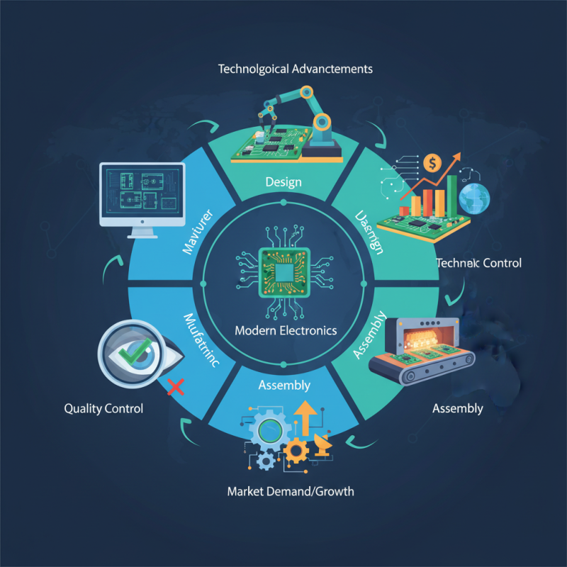
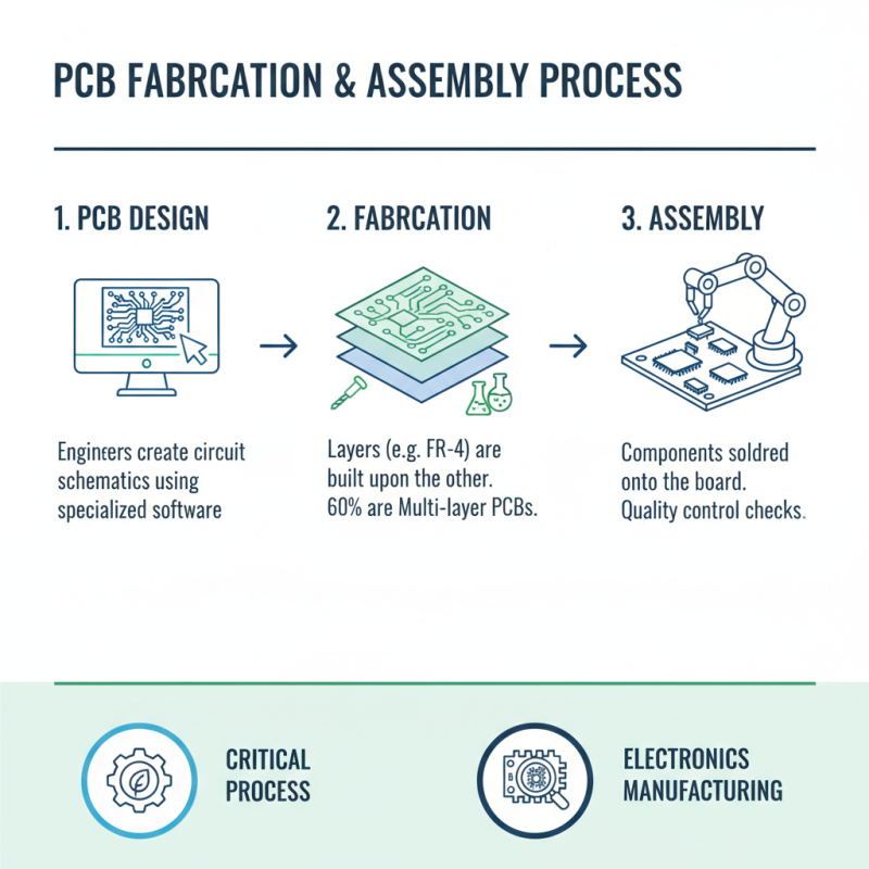
Overview of PCB Fabrication and Assembly Process
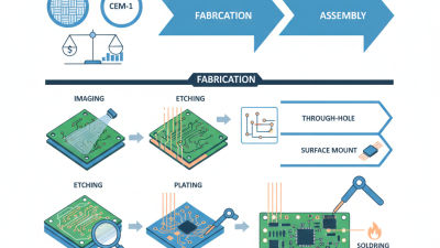
PCB fabrication and assembly is a critical process in electronics manufacturing. It begins with the design of the printed circuit board (PCB), where engineers input the intended circuit into specialized software. After design, the fabrication phase follows. This involves creating the PCB layers using materials like FR-4, a common type of fiberglass resin. Reports indicate that 60% of PCB production involves multi-layer PCBs, as they can support complex designs while saving space.
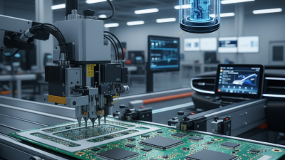
During assembly, surface mount technology (SMT) plays a crucial role. Components are placed on the board using automated machines. However, maintaining precision can be challenging. Consider that a mere 0.1 mm misalignment can lead to significant functionality issues. Industry studies show that around 15% of assembled boards may fail quality testing on their first pass. This highlights the need for rigorous inspection protocols. Despite advancements, imperfections still occur. Continuous improvement is essential in both fabrication and assembly to enhance yield rates and reduce waste.
Key Steps in PCB Design and Layout
In the PCB design process, layout is crucial. It involves arranging components and routing connections on the board. Designers must consider space and functionality. Each component must fit neatly on the board while maintaining accessibility. Planning is essential to avoid crowding or overlap. Often, layouts require adjustment and repetition. Trial and error can lead to valuable insights.
Understanding electrical signals helps in routing traces. Trace width impacts current capacity. Longer traces can introduce interference. Designers need to balance size with performance. Utilizing software tools aids in creating and modifying designs. However, software can become complex. Misunderstandings or errors may arise during the design phase. Testing layouts on prototypes is vital.
Layout design must account for manufacturing limitations. Designers often overlook these constraints. Small adjustments during the design can reduce costs later. Simple changes can enhance reliability. Components might interact unpredictably, leading to issues. Continuous reflection on design practices can improve future projects. Each PCB layout tells a story of balance, challenge, and learning.
What is PCB Fabrication and Assembly Process Explained? - Key Steps in PCB Design and Layout
| Step |
Description |
Tools Used |
Duration |
| 1 |
Design Schematic |
CAD Software |
1-2 Days |
| 2 |
PCB Layout |
PCB Design Software |
2-4 Days |
| 3 |
Protoype Fabrication |
CNC Machines, Laminators |
1-2 Weeks |
| 4 |
Component Placement |
Automated Pick and Place |
1-3 Days |
| 5 |
Soldering |
Reflow Oven, Wave Soldering |
1-2 Days |
| 6 |
Testing and Inspection |
Automated Test Equipment |
2-3 Days |
| 7 |
Final Assembly |
Manual Assembly Tools |
1-2 Days |
| 8 |
Packaging |
Packaging Equipment |
1 Day |
Materials Used in PCB Fabrication
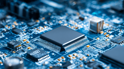
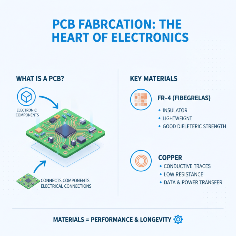
In the realm of electronics, PCB fabrication is crucial. A printed circuit board (PCB) connects various electronic components. The materials used in its fabrication impact performance and longevity. Common materials include FR-4, a type of fiberglass. It offers good electrical insulation and is lightweight. Copper is also widely used for the conductive traces on the board.
Another important component is solder mask, which protects against short circuits. It adds a layer of insulation over the copper traces. The selection of the solder mask color can vary; it may seem trivial but affects visibility during assembly. Additionally, surface finishes such as ENIG (Electroless Nickel Immersion Gold) ensure better solderability. While these materials are essential, the manufacturing process often reveals shortcomings in quality. Variations in thickness or impurities can lead to issues in the final product.
Revisiting the choice of materials is important. Not all materials work perfectly for every application. Designers often face challenges when balancing cost and performance. Some may overlook the importance of thorough testing. While familiar materials are a safe bet, innovation may require exploring new options. This experimentation can present its own set of challenges but can lead to better outcomes in PCB assembly.
PCB Fabrication Techniques Explained
PCB fabrication techniques are vital in electronics. The process transforms designs into functional circuits. Primarily, it involves etching, drilling, and layering materials. According to industry reports, the global PCB market is expected to reach $100 billion by 2025. This growth highlights the importance of understanding fabrication techniques.
One significant technique is subtractive etching. This method starts with a copper-clad board. Unwanted copper is removed, leaving the desired circuit pattern. It's effective and widely used. Yet, it can be wasteful. The precision required often leads to errors in complex designs. It's crucial to verify designs before production to minimize waste.
Tip: Always conduct thorough inspections of your PCB designs to avoid costly production mistakes. Another common technique is additive manufacturing. It builds layers of conductive material, offering unique design capabilities. However, it's still evolving and may not always meet high-volume demands. Designing for this method requires careful planning. It’s difficult to adapt designs once the fabrication process begins.
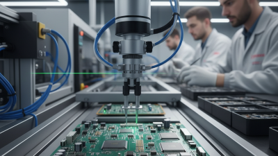
Assembly Methods for PCBs: Soldering and Testing
The assembly of printed circuit boards (PCBs) is crucial in electronics. Soldering is a primary method for connecting components. This process can either be manual or automated. Manual soldering is often used for small production runs. Automated soldering, like wave soldering, is better for large quantities. According to IPC-7525, approximately 90% of defects in solder joints can be traced back to human error during soldering.
Testing is as essential as assembly. After soldering, PCBs undergo various tests. Functional testing checks if all components work correctly. In-circuit testing looks for shorts or open circuits. A report from IPC states that effective testing reduces rework rates by 30%. Remember, a PCB that works perfectly during assembly can still fail in real-world conditions. Always consider rigorous testing.
**Tips:**
- Maintain a clean workspace. It reduces contamination.
- Regularly update soldering techniques based on current standards.
- Don't skimp on testing. It saves time and costs in the long run.
PCB Fabrication and Assembly Process: Soldering and Testing