How to Start PCB Fabrication Process in 2026?
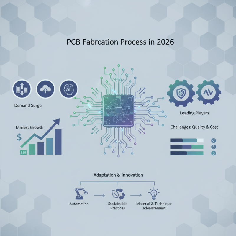
As the demand for electronics continues to surge, the PCB fabrication industry is experiencing significant growth. By 2026, the global PCB market is projected to reach $85 billion, driven by advancements in technologies such as IoT and AI. PCB fabrication is at the forefront, shaping how devices interact and perform.
Bosch and Infineon are leading players in the field, influencing trends and standards. For manufacturers, understanding the intricacies of PCB fabrication is crucial. Many newcomers overlook key factors in design and production. Quality assurance and cost management remain vital challenges.
In an evolving landscape, companies must adapt quickly. Improvements in materials and techniques are essential for staying competitive. Embracing automation and sustainable practices can enhance efficiency. Yet, many firms struggle to integrate these advancements. Identifying the right strategies is a continual process that requires reflection and growth. The future of PCB fabrication in 2026 depends on innovation and willingness to learn from past mistakes.
Understanding the Basics of PCB Fabrication and Its Importance
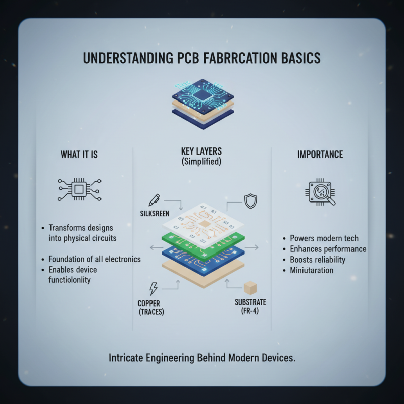
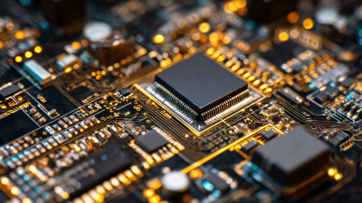
PCB fabrication is a crucial process in electronics manufacturing. It transforms circuit designs into physical boards that power countless devices. Understanding this process helps one appreciate the intricate engineering behind modern technology. Each layer of a PCB plays a specific role, from routing signals to supporting components. A well-designed board can enhance performance and reliability.
The importance of PCB fabrication lies in its ability to impact the overall product functionality. Flaws in fabrication can lead to device failures, which are costly. For instance, even a tiny misalignment of components can disrupt a device's operation. This is why attention to detail is key in the fabrication process.
As we look towards 2026, new materials and techniques will emerge. However, the fundamental principles will remain essential. Designers must stay informed about advancements. It’s a continuous learning journey. Mistakes are inevitable along the way, but they provide valuable lessons. Each experience can refine skills and lead to better outcomes in future projects.
Identifying Essential Tools and Materials Required for PCB Fabrication
The PCB fabrication process in 2026 requires careful preparation. You need specific tools and materials to succeed. A reliable soldering iron is essential. It allows precise connections without damaging components. Consider investing in a quality multimeter for testing electrical pathways. This tool helps ensure functionality in your final product.
You should also gather a PCB design software. This software enables you to create layouts effectively. A decent set of drill bits is necessary for creating holes accurately. Each hole must match the design. You may face challenges when aligning components. Patience is key here.
Lastly, don't overlook safety equipment. Protective eyewear and gloves will keep you safe during the process. Mistakes will happen, so be prepared for adjustments. Reflect on each step to improve as you go. This journey is about learning and refining your skills.
How to Start PCB Fabrication Process in 2026? - Identifying Essential Tools and Materials Required for PCB Fabrication
| Tool/Material |
Description |
Usage |
| Copper Clad Laminate |
Base material used for creating PCBs, coated with copper. |
Foundation for all PCB designs. |
| Etching Solution |
Chemical solution used to remove excess copper from the laminate. |
Used during the PCB manufacturing process to create circuits. |
| DRC Software |
Design Rule Check software to validate PCB designs. |
Ensures compliance with manufacturing constraints. |
| Solder Mask |
Layer of material that protects the copper from oxidation. |
Applied after etching to prevent solder from bridging. |
| Silkscreen Ink |
Used to print labels and other markings on the PCB. |
For component identification and assembly references. |
| Drilling Machine |
Machine used to create holes for components and vias. |
Essential for PCB assembly and functionality. |
| Multimeter |
Tool for measuring voltage, current, and resistance. |
Used for circuit testing and validation. |
| Hot Air Rework Station |
Tool to solder or desolder components on PCBs. |
Useful for assembling and repairing PCB components. |
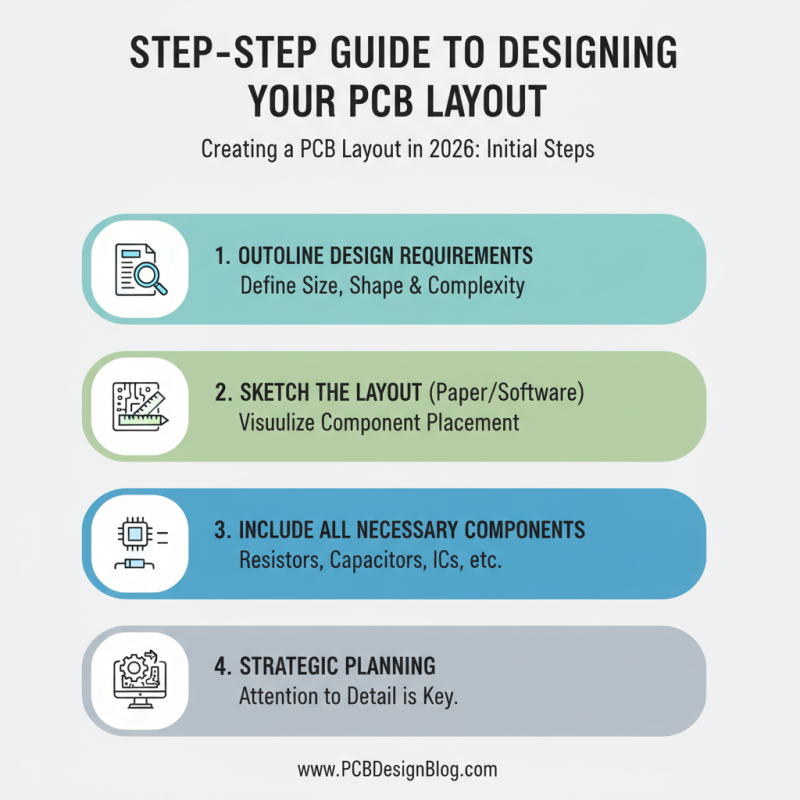
Step-by-Step Guide to Designing Your PCB Layout
Creating a PCB layout in 2026 requires strategic planning and attention to detail. Begin by outlining your design requirements. Determine the size, shape, and complexity of the PCB. Sketch the layout on paper or use software tools. Make sure to include all necessary components such as resistors, capacitors, and ICs.
Tips: It’s vital to keep component placement in mind. Try not to create cramped layouts. Ensure there’s ample space for traces and pads. Also, remember that larger traces carry more current. If you skip design rules, you may face fabrication issues later.
Once the initial design is set, review the connections. Routing traces accurately can be challenging. Be prepared to make adjustments. Check for signal integrity and avoid crossing traces. Utilize vias when needed but don’t overuse them. Remember that mistakes can add costs.
Tips: A peer review can provide fresh insights. Sometimes, you’re too close to your designs to spot errors. Get feedback early to save time later. Lastly, always save your work frequently. Losing progress can be frustrating and disruptive. Focus and reflect on your layout as enhancements are crucial for successful fabrication.
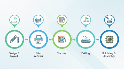
Navigating the Fabrication Process: From Artwork to Finished PCB
Starting the PCB fabrication process in 2026 requires careful planning and attention to detail. The journey begins with artwork creation, a crucial step that translates your design ideas into a visual format. This stage must ensure that the layouts comply with specific industry standards. High-resolution images are essential since even minor errors can lead to expensive reworks later on. According to a 2023 industry report, 45% of PCB defects stem from design flaws, underlining the significance of this initial phase.
Once the artwork is ready, the actual fabrication can begin. This involves multiple steps, including etching, drilling, and layering. Each step has its own set of challenges. For example, precision in drilling is essential, as even a slight deviation can cause failures. Data shows that 30% of delayed projects are due to fabrication errors. It's critical to maintain open communication with fabrication teams throughout this process. Regular feedback can prevent miscommunications and lead to better final products.
Ultimately, the transition from concept to a finished PCB is often less linear than expected. Challenges arise unexpectedly. You must be prepared for setbacks. Keeping an adaptable mindset will help you learn and adjust. Embracing a mindset of continuous improvement contributes to better outcomes in the long run. The path may have its flaws, but acknowledging them is part of mastering the PCB fabrication process.
Quality Control Measures in PCB Manufacturing and Testing
Quality control is crucial in PCB manufacturing. It ensures that each component functions as designed. The process begins with design validation. Engineers check the PCB layout against specifications. Mistakes at this stage can lead to costly errors later.
Testing follows fabrication. Methods like automated optical inspection (AOI) identify defects. These defects can include misaligned traces or solder issues. Even small errors may result in significant failures. Regular calibration of testing equipment is also necessary. This helps maintain accuracy.
Quality control measures should not be seen as just checkboxes. They require continuous improvement and adaptation. Feedback from testing helps refine processes. Workers need training in spotting potential flaws. There is always room for enhancement. Each inspection should be viewed as an opportunity to learn. Being vigilant in quality control can elevate overall production standards.
PCB Manufacturing Quality Control Measures