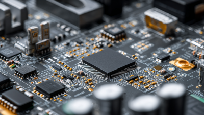
Top Trends in Fast PCB Prototyping for 2025 You Need to Know
As we look ahead to 2025, the landscape of fast PCB prototyping is evolving at an unprecedented pace, driven by technological advancements and the increasing need for rapid product development. Industry expert Dr. Emily Chen, a renowned figure in PCB manufacturing, emphasizes the urgency of staying updated in this field, stating, "The future of fast PCB prototyping will hinge on our ability to innovate quickly and efficiently." Her insights highlight the critical role that speed and flexibility will play in the success of businesses navigating this competitive terrain.
In the coming years, several trends are poised to redefine fast PCB prototyping. These include the integration of AI-driven design tools, advancements in material science, and the rise of cloud-based collaboration platforms. Such innovations promise to streamline the prototyping process, significantly reducing lead times while enhancing product quality. As we delve into these trends, it becomes clear that embracing these changes is not just advantageous but essential for companies aiming to maintain a competitive edge.
Understanding these dynamics will not only prepare businesses for the future of fast PCB prototyping but also inspire them to innovate and adapt in an ever-changing market. By focusing on these emerging trends, organizations can position themselves effectively, ensuring they are well-equipped to meet the demands of tomorrow's technology landscape.

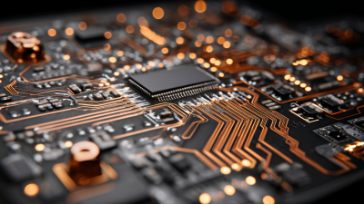
Key Drivers of Fast PCB Prototyping Innovation in 2025
The landscape of PCB prototyping is evolving rapidly, driven by technological advancements and market demands. As we approach 2025, several key drivers are poised to reshape the fast PCB prototyping industry. First and foremost, the increasing complexity of electronic devices requires PCB designs to evolve swiftly. The rise of IoT and smart technology necessitates rapid iterations and shorter lead times to stay competitive. This has led to an emphasis on automation and digital tools that streamline the design and prototyping processes.
Another significant driver of innovation in fast PCB prototyping is the adoption of advanced materials. Engineers are now exploring new substrates that offer enhanced performance, reliability, and flexibility. These materials not only support high-frequency applications but also enable miniaturization, meeting the demands of modern electronic components. As a result, fast prototyping methods are being refined to accommodate these advanced materials, allowing for more sophisticated designs to be tested and produced quickly.
**Tip:** When engaging in PCB prototyping, always consider the material requirements early in the design phase. This foresight can prevent delays later in production.
Furthermore, the rise of AI and machine learning is revolutionizing the prototyping process by optimizing design workflows and predicting potential issues before they arise. These technologies facilitate data analysis, enabling engineers to make informed decisions in real-time. The integration of cloud-based platforms also allows for collaboration across different teams and geographic locations, enhancing innovation speed and efficiency.
**Tip:** Leverage collaborative tools that utilize cloud technology to streamline communication and improve prototype iterations among team members.
Top Trends in Fast PCB Prototyping for 2025 You Need to Know
| Trend |
Key Drivers |
Impact on Prototyping |
Estimated Growth (%) |
| AI Integration |
Enhanced design accuracy and speed |
Faster turnaround times and reduced errors |
30% |
| 3D Printing |
Lower material costs and rapid prototyping |
Shorter development cycles |
25% |
| Cloud-Based Prototyping |
Remote collaboration and resource sharing |
Increased accessibility and flexibility |
20% |
| Flexible PCB Designs |
Rising demand for compact and lightweight devices |
Broader applications in electronics |
15% |
| Automated Workflow |
Efficiency improvements through automation |
Reduced lead times and costs |
35% |
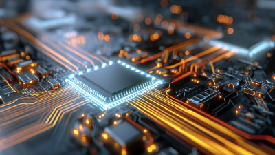
Emerging Technologies Impacting PCB Prototyping Speed and Efficiency
Emerging technologies are fundamentally reshaping the landscape of PCB prototyping, paving the way for faster and more efficient design processes. One of the most notable advancements is the adoption of artificial intelligence (AI) and machine learning algorithms, which optimize design layouts and automate error detection. By analyzing vast amounts of data, these technologies can predict potential issues before they arise, significantly reducing the time engineers spend on revisions.
Moreover, additive manufacturing, commonly known as 3D printing, is gaining traction in PCB prototyping. This technique allows for rapid iteration of designs, enabling creators to test multiple variations without the lengthy delays associated with traditional manufacturing methods. As 3D printing continues to evolve, it is likely to decrease costs while enhancing flexibility in material choices and design capabilities.
Tips: When considering new technologies for PCB prototyping, it's essential to keep an eye on the latest software updates that integrate AI capabilities. Additionally, investing in training for your team on 3D printing techniques can drastically shorten development cycles. By staying informed and prepared, you can capitalize on these emerging trends to accelerate your product development process.
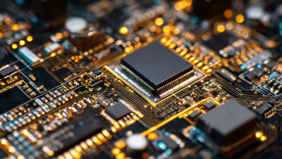
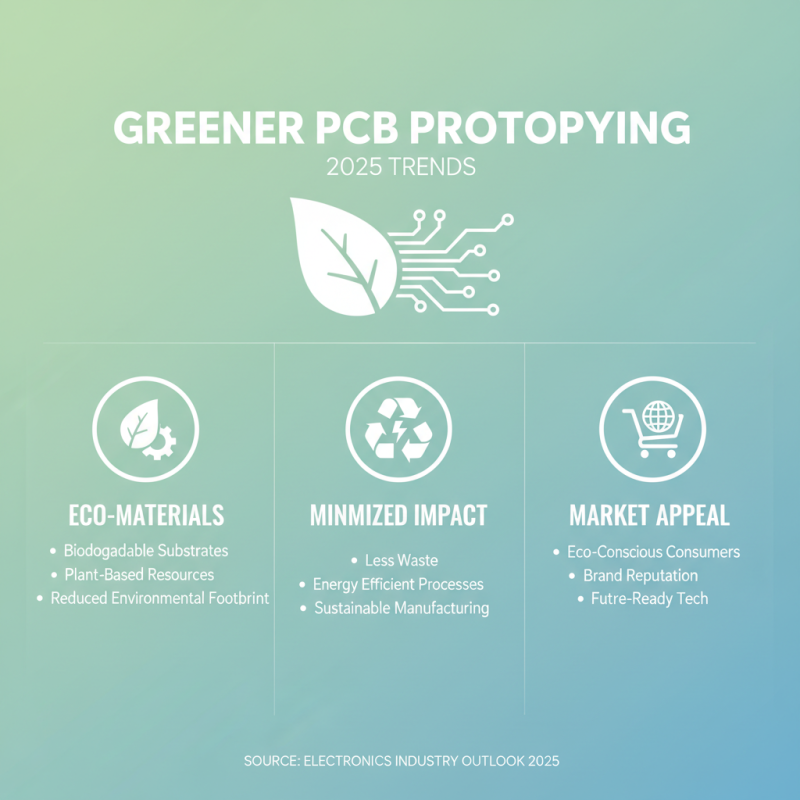
Sustainability Trends in PCB Prototyping for Future Applications
As the electronics industry moves towards a greener future, sustainability trends in PCB prototyping are becoming increasingly prominent. In 2025, manufacturers are expected to prioritize eco-friendly materials and processes that minimize waste and energy consumption. Biodegradable substrates, such as those derived from plant-based resources, are emerging as viable alternatives to traditional materials. These innovations not only enhance the environmental footprint of PCB production but also appeal to a market that is becoming more environmentally conscious.
Additionally, the adoption of advanced manufacturing technologies, such as additive printing, will further drive sustainability in PCB prototyping. These techniques reduce material waste by allowing for precision in design and production, creating only what is necessary. Moreover, processes that utilize renewable energy sources during production are gaining traction, signaling a shift in the industry towards greener practices. As companies aim to enhance their sustainability profiles, the integration of closed-loop systems in PCB recycling can provide a pathway to reusing valuable materials, thereby fostering a circular economy in electronics.
Market Demand and User Expectations Shaping PCB Prototyping
The landscape of PCB prototyping is rapidly evolving, driven by increasing market demand and the ever-changing expectations of users. As electronics become more integrated into everyday products, the need for faster and more efficient prototyping processes has never been greater. Users expect prototypes to not only be delivered quickly but also to incorporate advanced functionalities and accommodate tighter tolerances. This shift is prompting manufacturers to innovate their methodologies, integrating automation and digital tools to streamline the design and production cycles significantly.
Furthermore, sustainability is emerging as a crucial factor in PCB prototyping. Users are increasingly concerned about the environmental impact of manufacturing processes and materials. This expectation is steering the industry toward greener practices, including the use of eco-friendly materials and energy-efficient production techniques. As a result, these trends are reshaping the development of prototypes, with a growing emphasis on lifecycle assessments and recycling initiatives. Consequently, companies that align with these user expectations are poised to gain a competitive edge in an increasingly eco-conscious market.
Best Practices for Adopting Fast PCB Prototyping Techniques in 2025
As we move into 2025, organizations aiming to enhance their product development processes must prioritize adopting fast PCB prototyping techniques. One of the best practices involves implementing agile methodologies. By adopting an iterative approach, teams can refine designs through multiple prototypes, allowing for faster feedback loops and minimizing time spent on revisions. This ensures that each iteration aligns more closely with project goals and user requirements.
Moreover, investing in advanced software tools that facilitate quick design iterations is crucial. These tools often include features such as real-time simulation and automatic design rule checks, enabling engineers to identify potential issues early in the design phase. Furthermore, leveraging cloud-based collaboration platforms can enhance communication among team members, ensuring that everyone is aligned and can contribute to the prototyping process seamlessly. By integrating these practices, companies can significantly reduce their time-to-market while maintaining high standards of quality and innovation.
Top Trends in Fast PCB Prototyping for 2025