Blog

2026 Top Types of PCB Manufacturing and Assembly?

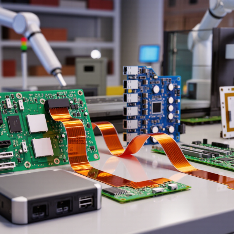
PCB manufacturing and assembly will look more specialized in 2026. Product designers now balance electrical performance, production volume, repairability, and environmental demands. The best choice depends on the device, not on a popular process name. Rigid PCBs remain common in industrial controls, appliances, and computing equipment. Flexible circuits fit cameras, medical wearables, and compact hinges. Rigid-flex boards combine stability with controlled bending. HDI technology supports smaller products through fine traces, microvias, and dense component placement. Metal-core boards help transfer heat from high-power LEDs and converters. Ceramic substrates serve demanding thermal and high-frequency applications, although their cost can limit wider adoption.

Assembly choices matter just as much. Surface-mount technology supports compact layouts and automated placement. Through-hole assembly still offers valuable mechanical strength for connectors, switches, and heavy components. Mixed-technology assembly is often practical when one board contains both tiny ICs and rugged terminals. Prototype assembly may prioritize speed and engineering feedback. High-volume production usually requires tighter process control, automated inspection, and stable supply planning. Turnkey manufacturing can simplify sourcing, but it still requires transparent documentation and supplier verification. Check the details.

Experienced teams inspect solder joints with SPI, AOI, and, when necessary, X-ray analysis. They also review stackups, thermal paths, tolerances, and test coverage before release. Yet no process is flawless. A cheaper board may create hidden assembly risks. A technically advanced design may become difficult to repair. This guide compares leading PCB manufacturing and assembly types, using practical criteria rather than marketing claims. Some recommendations remain judgment calls, and that uncertainty deserves honest attention.

2026 Top Types of PCB Manufacturing and Assembly?

What PCB Manufacturing and Assembly Mean in 2026

In 2026, PCB manufacturing means converting a verified circuit design into a reliable physical board. It includes material selection, imaging, copper plating, drilling, solder-mask application, and electrical testing. Common types include rigid, flexible, rigid-flex, high-density interconnect, and metal-core boards. Each type serves a different need, from compact wearables to heat-producing power systems.

PCB assembly means placing and joining components onto that board. Surface-mount technology supports small, dense layouts, while through-hole assembly adds mechanical strength for larger parts. Modern factories often combine automated placement, controlled reflow, optical inspection, and selective soldering.

During production reviews, I have found that tiny details matter. A warped panel or poorly stored component can create failures weeks later. No process is perfect. Design files also need honest review, not blind trust.

Tips:

Confirm stack-up materials, copper thickness, tolerances, and assembly limits before ordering. Request sample testing and clear inspection records. Check component availability early, because substitutions can alter footprints or electrical behavior. Keep revision history visible. A neat board is not automatically a dependable board. Reliability comes from traceable materials, stable processes, functional testing, and careful engineering decisions. Teams should also examine repair access, thermal performance, and end-of-life handling. These points are sometimes overlooked when schedules become tight.

Which PCB Types Are Used in Modern Electronics

Modern electronics rely on several PCB types, each chosen for its electrical, mechanical, and thermal demands. Rigid PCBs remain common in computers, appliances, and control equipment. Their solid fiberglass structure supports stable component placement and automated assembly. Flexible PCBs bend around hinges, cameras, and wearable devices. They reduce wiring volume and tolerate repeated movement. Rigid-flex boards combine both advantages, although their fabrication requires careful layer alignment and bend-radius control.

High-density interconnect boards support compact products with limited internal space. Microvias and fine traces connect processors, memory, and sensors without enlarging the board. Multilayer PCBs also improve routing by separating power, signals, and ground planes. In high-temperature equipment, metal-core boards help move heat away from LEDs or power components. Ceramic boards offer excellent thermal stability, but they can be more expensive and less forgiving during handling.

Assembly choices must match the PCB structure. Surface-mount assembly suits dense layouts, while through-hole parts can provide stronger mechanical support for connectors. Inspection should check solder joints, warpage, hidden vias, and thermal interfaces. No board type is perfect. A flexible circuit may solve space problems but complicate repair. A high-density design can reduce size but increase manufacturing sensitivity. In practice, engineers sometimes choose a familiar structure too early. Reviewing heat, vibration, bending, service access, and production volume together usually produces a more reliable decision.

2026 Top Types of PCB Manufacturing and Assembly? - Which PCB Types Are Used in Modern Electronics

PCB Type Typical Construction Common Layer Range Manufacturing Characteristics Suitable Assembly Methods Typical Applications Main Benefits and Limitations
Single-Sided PCB One conductive copper layer on one side of an insulating substrate, usually with through-hole or surface-mounted components on the same side. 1 copper layer The simplest and most economical PCB structure; routing is limited because conductive traces cannot cross on the same layer. Through-hole assembly and basic surface-mount assembly. Power supplies, LED lighting, calculators, basic control panels, and low-complexity consumer products. Benefits: low cost, simple fabrication, fast production.
Limitations: low routing density and limited circuit complexity.
Double-Sided PCB Copper layers on both sides of the dielectric substrate, connected through plated through-holes or other vias. 2 copper layers Supports more routing than a single-sided board and allows components to be placed on both sides. Through-hole, single-sided SMT, or double-sided SMT assembly. Industrial controls, automotive modules, instrumentation, appliances, and moderate-complexity electronics. Benefits: improved routing density and design flexibility.
Limitations: higher cost and more complex fabrication than single-sided boards.
Multilayer PCB Three or more conductive layers separated by dielectric materials and laminated into one board, commonly including dedicated power and ground planes. 4–32+ copper layers, depending on design complexity Requires layer alignment, lamination, controlled impedance, and accurate via formation; fabrication yield becomes more sensitive as layer count rises. High-density SMT, fine-pitch component placement, through-hole, and mixed-technology assembly. Servers, networking equipment, medical systems, industrial automation, aerospace electronics, and advanced embedded systems. Benefits: high density, better signal integrity, compact form factor.
Limitations: higher manufacturing cost, longer design verification, and more difficult rework.
Rigid PCB A non-flexible laminated board made from a rigid substrate, commonly using glass-reinforced epoxy materials. 1–32+ layers Provides stable mechanical support and predictable dimensions for automated component placement and enclosure mounting. Automated SMT, through-hole, mixed-technology, and selective soldering. Computers, communication equipment, industrial controllers, appliances, automotive electronics, and test instruments. Benefits: strong, dimensionally stable, and widely available.
Limitations: cannot bend during use and may require connectors between separate rigid sections.
Flexible PCB Thin copper traces formed on flexible polymer film, allowing the circuit to bend or fold during installation and operation. 1–8+ layers Uses flexible coverlay materials, bend-radius rules, and strain-relief design; dynamic flexing requires additional mechanical validation. Surface-mount, microvia, anisotropic conductive bonding, and selective through-hole assembly. Wearable devices, cameras, displays, medical instruments, compact sensors, and space-constrained electronic assemblies. Benefits: lightweight, thin, bendable, and reduces wiring and connectors.
Limitations: higher material and assembly cost, with tighter bend and handling requirements.
Rigid-Flex PCB A combined structure containing rigid sections interconnected by flexible PCB sections within one integrated assembly. Typically 4–20+ layers across rigid and flex sections Combines rigid-board routing with controlled flex zones; requires careful stack-up, bend, lamination, and transition design. High-density SMT, through-hole assembly on rigid areas, and specialized flex handling during assembly. Aerospace systems, medical equipment, automotive electronics, robotics, and compact handheld products. Benefits: fewer connectors, improved reliability, and better three-dimensional packaging.
Limitations: high design complexity, higher cost, and more demanding inspection.
HDI PCB High-density interconnect board using fine traces, small pads, microvias, and sequentially built-up dielectric layers. Usually 4–16+ layers Uses laser-drilled microvias, fine-line imaging, and sequential lamination to increase interconnect density and shorten signal paths. Fine-pitch SMT, micro-BGA, chip-scale packages, and advanced automated placement. Mobile electronics, compact computing devices, medical wearables, cameras, and high-density control systems. Benefits: smaller products, higher routing density, and improved electrical performance.
Limitations: tight process control, higher cost, and more demanding design rules.
Metal-Core PCB A metal base, commonly aluminum or copper, combined with a dielectric layer and copper circuit layer for heat spreading. Usually 1–2 copper layers Designed around thermal resistance, dielectric thickness, metal-core flatness, and heat dissipation requirements. Surface-mount assembly, thermal-pad reflow, and high-power component attachment. LED luminaires, automotive lighting, power converters, motor control, and thermal-intensive electronic modules. Benefits: improved thermal management and mechanical rigidity.
Limitations: limited multilayer capability and more difficult drilling, routing, and rework.
High-Frequency PCB A PCB using low-loss, controlled-dielectric materials and carefully engineered transmission-line geometries. 2–16+ layers Requires controlled impedance, precise dielectric thickness, low-loss materials, smooth copper, and strict signal-integrity control. Fine-pitch SMT, RF connectors, shielded assembly, and automated placement with controlled soldering profiles. Wireless communication, radar, satellite equipment, antennas, test instruments, and high-speed data systems. Benefits: supports high-frequency and high-speed signal transmission.
Limitations: higher material cost and strong sensitivity to layout, fabrication tolerances, and surface finish.
Ceramic PCB Conductive circuits formed on or within a ceramic substrate, offering strong electrical insulation and thermal performance. 1–10+ layers, depending on ceramic technology Ceramic processing supports high-temperature operation and thermal expansion compatibility with certain power semiconductor packages. Surface-mount, wire bonding, die attach, and high-temperature component assembly. Power electronics, high-temperature sensors, laser systems, automotive modules, and aerospace equipment. Benefits: excellent thermal stability, insulation, and dimensional reliability.
Limitations: brittle substrate, specialized processing, and higher cost.
Embedded-Component PCB Passive or semiconductor components are placed inside the PCB structure rather than only on its outer surfaces. 4–20+ layers Requires component embedding, precise lamination, thermal analysis, and inspection methods capable of verifying internal structures. Mixed automated assembly, surface-mount assembly, and specialized embedded-component processes. Miniaturized modules, high-density computing, medical electronics, automotive systems, and advanced sensor platforms. Benefits: smaller footprint, shorter electrical paths, and improved packaging density.
Limitations: difficult inspection, repair, thermal analysis, and manufacturing process control.

Note: Layer counts and manufacturing characteristics are representative industry ranges. Actual capabilities depend on the material system, design rules, reliability requirements, and production process.

How PCB Manufacturing Processes Differ by Board Type

2026 Top Types of PCB Manufacturing and Assembly

How PCB Manufacturing Processes Differ by Board Type

PCB manufacturing changes sharply with the board’s structure, not just its size. Rigid multilayer boards usually use copper etching, mechanical drilling, lamination, plating, and automated optical inspection. Flexible circuits need thinner copper, coverlay, tighter bend-radius control, and stress testing. Rigid-flex boards add staged lamination, because flexible and rigid materials expand differently under heat. HDI boards rely on sequential buildup, laser microvias, and precise registration. Small errors can multiply.

Assembly also follows the board type. Standard rigid boards commonly support high-speed surface-mount placement and selective through-hole soldering. Flex assemblies need low-stress handling and temporary carriers. Metal-core boards require thermal interface checks before component placement. According to Grand View Research’s 2024 PCB market analysis, the global market was valued at about USD 89.7 billion in 2023, with continued growth expected through 2030. That growth does not make every process interchangeable. A cheaper process can create expensive rework.

Tips: Match the stack-up to the operating environment. Review bend cycles, heat paths, via structures, and inspection access before ordering tooling. IPC design guidance can support this review, but it cannot replace a pilot build. Production teams often discover that simulation misses fixture pressure or uneven copper distribution. A perfect yield model is rare. Leave room for measurement, correction, and one uncomfortable question: is this board type genuinely necessary?

How PCB Assembly Methods Support Different PCB Designs

2026 Top Types of PCB Manufacturing and Assembly

How PCB Assembly Methods Support Different PCB Designs

PCB assembly methods should follow the board’s physical and electrical demands. Surface-mount technology suits compact designs with dense component placement. It supports short signal paths and automated, repeatable production. Through-hole assembly adds stronger mechanical joints for connectors, switches, and heavy components. It needs more board space, but that space can improve durability.

Mixed assembly combines both methods on one PCB. This approach works well when a small controller sits beside large power terminals. Flexible and rigid-flex boards also require careful component placement. Heavy parts may stress bending areas during use. Engineers should review heat, vibration, access for inspection, and repair conditions before selecting an assembly process. No method is perfect. A compact design may still become difficult to service.

Tips: Match component size to assembly limits. Keep tall parts away from bend zones. Leave inspection access around critical joints. Use prototypes to test thermal behavior and mechanical fit. Do not trust software checks alone; a board can pass layout rules and still be awkward to assemble. Experienced technicians often notice these practical problems during the first build. That feedback should influence the next revision. It may feel inefficient, but early changes usually cost less than repeated production corrections.

2026 Top Types of PCB Manufacturing and Assembly

How PCB assembly methods support different PCB designs

The chart uses a practical engineering suitability index from 0 to 5, where 5 indicates strong compatibility with the PCB design type. SMT is widely suited to high-density, multilayer, and HDI boards; through-hole assembly is commonly selected for mechanically robust or high-power components; and mixed-technology assembly combines both approaches when a design contains surface-mount and through-hole parts. Flexible and rigid-flex boards usually require controlled handling, support fixtures, and specialized process settings.

How to Select the Right PCB Manufacturing and Assembly Option

How to Select the Right PCB Manufacturing and Assembly Option

Choosing a PCB process begins with the product, not the factory quotation. A simple sensor may need a single-sided or double-sided rigid board. Dense computing hardware may require multilayer construction, controlled impedance, or HDI features. Flexible and rigid-flex boards suit cameras, wearables, and devices with repeated movement. Assembly choices also matter. Surface-mount technology supports compact designs and high volume. Through-hole assembly adds mechanical strength for connectors and large components. Mixed assembly is often practical, but it can increase inspection and handling requirements.

Tips: Match the process to volume, tolerance, materials, and testing needs. Request a design-for-manufacturing review before ordering. Ask how solderability, warpage, component availability, and trace spacing will be checked. Confirm electrical tests, visual inspection, and sample approval procedures. A clear inspection plan prevents expensive surprises.

In project reviews, I have seen a low unit price hide setup fees, slow rework, or costly minimum orders. Lead time should include fabrication, component sourcing, assembly, and testing. Ask for realistic dates, not optimistic promises. Your board may need high-temperature laminate, fine-pitch placement, or heavy copper for power paths. These details change the suitable process. I still find early assumptions are sometimes wrong. A prototype may pass electrically but fail during vibration or thermal cycling. Build a small pilot batch, record defects, and adjust the design before full production. Reliability grows from evidence, not confidence alone.