What Is PCBA Manufacturing and How Does It Work?
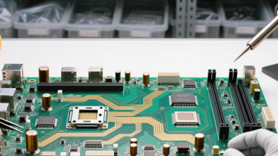
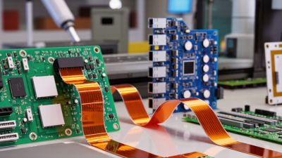
PCBA manufacturing turns a bare printed circuit board into an assembly that performs a defined electronic task. The process combines component sourcing, soldering, inspection, and testing, with each step affecting reliability. A board may pass through solder paste printing, pick-and-place machines, and a reflow oven before technicians inspect its joints. Small details matter: paste volume, component alignment, and oven temperature can affect whether a connection holds under use. Details matter. This is practical production, not just a sequence of machines. It requires controlled procedures and decisions based on the design, materials, and expected operating conditions.
Understanding how pcba manufacturing works helps product teams ask better questions about cost, lead time, and quality. The exact route depends on board complexity. A simple prototype may be assembled by hand, while a dense production panel needs automated placement and documented process controls. Inspection can include optical systems, X-ray imaging for hidden solder joints, and electrical tests for opens or shorts. Tests have limits. Results must be checked against product requirements, and failures should prompt investigation rather than quick assumptions. Even a well-managed line can encounter variation, so traceability, clear work instructions, and realistic yield targets matter. This guide explains the main stages, common methods, and choices behind dependable assembly. It also considers an important caveat: the most advanced process is not always the best fit.
What PCBA Manufacturing Means and How It Differs from PCB Fabrication
What Is PCBA Manufacturing and How Does It Work?
PCB fabrication creates the bare board: a nonconductive panel with copper traces, drilled holes, and protective finishes. PCBA manufacturing begins after that. It adds components and turns the board into an assembled electronic unit. In plain terms, fabrication makes the “roads”; assembly installs the parts that use them. They are related stages, but not interchangeable.
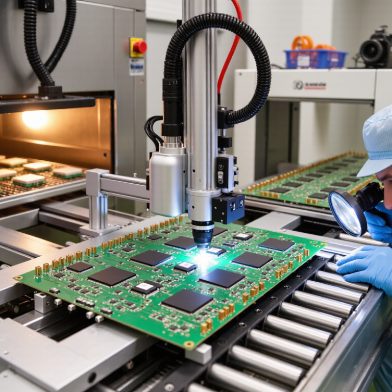
A typical PCBA line applies solder paste through a stencil, places surface-mount parts, and sends the board through a controlled reflow oven. Larger components may be inserted and soldered separately. Technicians then inspect solder joints, often with automated optical inspection or X-ray for hidden connections. Functional testing can check whether the assembled board behaves as intended. Small details matter: paste volume, component alignment, and oven temperature can all affect reliability.
The scale is substantial. Prismark’s 2024 PCB Industry Report estimated global PCB production value at about US$68.3 billion in 2023, reflecting the breadth of the fabrication supply chain. That figure does not represent PCBA alone. It is a useful distinction. A bare board can pass fabrication inspection yet fail after assembly, so quality checks must cover both stages. A clean process map helps, but it can hide the real challenge: matching board design, components, and production controls before defects reach the test bench.
What Materials and Components Are Needed for PCBA?
A PCBA combines a bare printed circuit board with the components that perform its electrical functions. The board commonly uses FR-4, a glass-fiber and epoxy laminate, with copper foil forming conductive traces. Solder mask covers most copper, while silkscreen marks component locations and polarity. Small details matter.
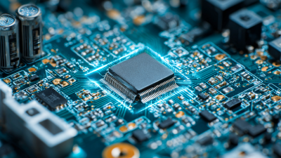
Components may include resistors, capacitors, integrated circuits, connectors, and sensors. Their packages must match the board’s footprint and assembly process. Solder paste, usually a metal alloy mixed with flux, temporarily holds surface-mount parts before reflow. Through-hole parts may use solder wire or selective soldering. Not every board needs every material.
Material selection affects cost, durability, and heat handling. The USGS Mineral Commodity Summaries 2024 estimated global copper mine production at about 22 million metric tons in 2023. That figure is not PCBA-specific, but it shows why copper availability matters to electronics supply chains. For a real design, check the board’s current, temperature, and operating environment before choosing copper thickness or laminate. FR-4 is common, not universal. A rushed material choice can make a board harder to assemble or less reliable; even the right components need compatible pads, solder, and thermal limits.
How Bare Boards Are Prepared for Component Assembly
Before components arrive, each bare board needs a careful incoming check. Technicians compare its outline, dimensions, and layer details with the fabrication data. Under bright light or magnification, they look for scratches, lifted solder mask, blocked holes, and uneven copper pads. A tiny smear matters. Boards with contamination can cause poor solder joints later, even when the assembly process is well controlled.
The board is then cleaned using a process suited to its surface finish and materials. It must be dried and handled by its edges to reduce oils and dust. Baking may be appropriate for some boards, but only when the material supplier’s guidance supports it; excess heat can cause damage. Technicians also check flatness, since a warped panel can shift during printing. Fiducial marks and tooling holes help align the board with the solder-paste stencil and assembly equipment.
Before components are placed, the board is secured on a support, and the stencil is aligned over its pads. A first print is inspected for paste coverage, smears, and blocked apertures. Small adjustments can prevent misaligned deposits from becoming solder defects. This step is not foolproof: inspection samples only part of the process, so clean handling and consistent setup remain important.
How Components Are Mounted and Soldered onto the Board
PCBA manufacturing turns a bare circuit board into a working assembly by placing and soldering components in a controlled sequence. For surface-mount parts, a stencil spreads solder paste across small copper pads. Automated pick-and-place equipment positions resistors, capacitors, and chips on the tacky paste. A misplaced component can look almost correct, yet still create an open circuit.
The board then passes through a reflow oven, where carefully controlled heat melts the paste and forms solder joints. Temperature profiles depend on the board and component mix; one setting does not suit every assembly. The WSTS Spring 2024 Forecast projected semiconductor sales of $611.2 billion for 2024, reflecting the scale and variety of parts that assembly lines must handle. After reflow, optical inspection checks alignment and visible solder defects. It cannot reveal every hidden joint, so X-ray inspection may be needed for packages with connections underneath. Through-hole components follow a different route: their leads enter drilled holes and are soldered by wave or selective soldering. IPC J-STD-001 provides workmanship requirements, but inspection still needs sound judgment. It is not foolproof. Tiny process changes can matter.
How PCBA Inspection and Testing Verify Board Performance
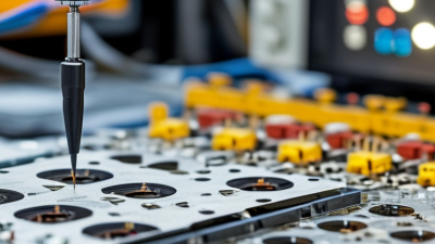
In PCBA manufacturing, inspection checks whether components are correctly placed and soldered before a board moves into service. Operators may use magnification to examine fine-pitch pins, solder joints, and connector alignment. Automated optical inspection compares board images with design data and can flag missing parts or uneven solder. Small defects matter.
Visual checks cannot reveal everything. X-ray inspection can help assess hidden joints beneath packages, while in-circuit testing checks electrical connections and component values at selected points. Functional testing then powers the assembled board and checks whether key outputs match expected behavior. Test limits should reflect the board’s real operating requirements, not just convenient measurements.
A useful inspection plan combines these methods according to board complexity, risk, and production volume. Test logs, defect photos, and repair records help teams trace recurring problems, such as a shifted component or inconsistent soldering. Still, a passing test is not a promise of perfect field performance. Some faults appear only under heat, vibration, or extended use. That gap deserves attention. Reviewing failures from real use can help refine test coverage and improve the next production run.
How PCBA Inspection and Testing Verify Board Performance
A functional test can monitor a board’s power rail while the circuit is operating under load. These illustrative readings show a 3.3 V rail remaining within a sample ±5% range; actual acceptance limits depend on the board design. Visual inspection, automated optical inspection, X-ray inspection, and in-circuit testing can check assembly quality and electrical connections before or alongside functional testing.